 |
248 MARF
Multiple
Arbitrary |
|
V2 modifications to reduce CV jitter, operate with the expander, fixes and enhancements are located on the V2 modifications page.
V1
I have built and repaired the 248 MARF V1. The module is a total redesign with a microprocessor and is quite complex.
I cleaned up the 1977 manual and the brochure from the scans on the Magnus site and formatted them as PDFs.
The build is fairly fast as only the panel components need to be assembled but V1.0 does require a number of SMT modifications. Programming and calibration is straightforward.
The V1.0 PCBs have several SMT resistor and capacitor parts to be changed on the front and rear. The silk screen is difficult to read and I have helped several people repair their MARFs when they changed the wrong parts. These two reference diagrams highlight in color the required component to modify.
MARF V1.0 front component changes
MARF V1.0 rear component changes
Calibration
Calibration is straightforward.
Multiplier, Address, and External CV Inputs:
The Time Multiplier and Address controls may NOT work until you have performed this calibration. Don't panic if these controls don't work at first turn on.
To calibrate the Time Multiplier and Address controls and the CV inputs turn all four controls fully CW. Hold the left Advance switch down while turning on the power. The green/yellow/red LEDs should begin to cycle. Release the Program 1 Advance switch. Apply 10.0V into all four external inputs. Then press the Program 2 Advance switch down. The LEDs will stop cycling and your controls and 10V inputs are now calibrated.
Volts/Octave Output:
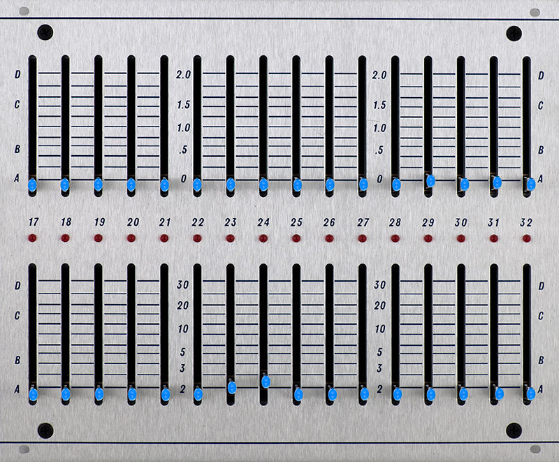
Set the DIP switches for 2V/Octave. Set all the sliders to minimum.
Program 1: Connect a DMM to the Voltage Output, set the Cont/Strobe to center, press the Display switch, Stop switch, Reset switch, and +0 limited switch. The DMM should now read some low mV voltage. Record this voltage for the next step.
Press the +2 limited switch and adjust the front panel trimmer next to the Time Multiplier knob for 2.0 volts plus whatever the recorded low mV voltage was. Now check the accuracy at the +4, +6 and +8 settings. Readjust if necessary. You want the increment for the switches to be +2, +4, +6, or +8 volts so this voltage above the 0V measurement.
Program 2: Perform the same procedure with the Program 2 controls and outputs.
CV Jitter
See below under V2.
Epilog
PM on Modwiggler has developed V1.6 to address a number of issues and his code is posted on the thread MARF 248 New Firmware Announcement page. I do not have a V1 but have been trying to help individuals with V1 by email. I have a 248 V1 Modifications to try and document it all in one place.
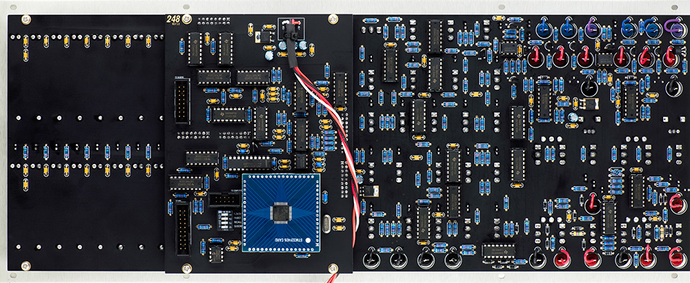
V2
V2 modifications to reduce CV jitter, operate with the expander, fixes and enhancements are located on the V2 modifications page.
Expander modifications to operate with V2 are also located on the V2 modifications page.
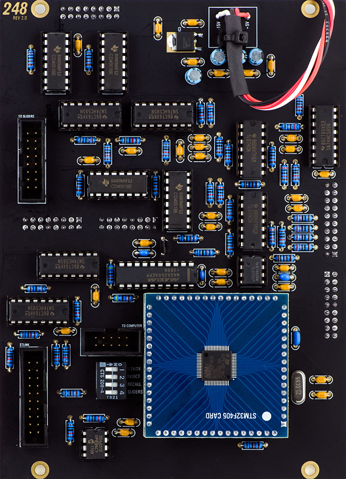
This V2 description is for the ElectricMusicStore PCBs.
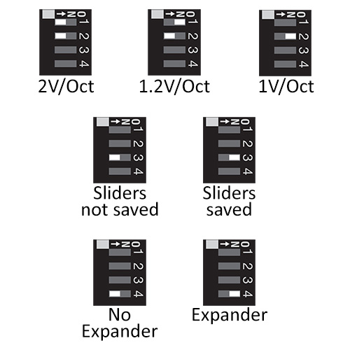
The V/Oct DIP switch settings are wrong in the manual. This illustration shows the correct DIP switch settings.
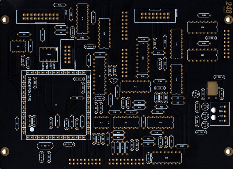
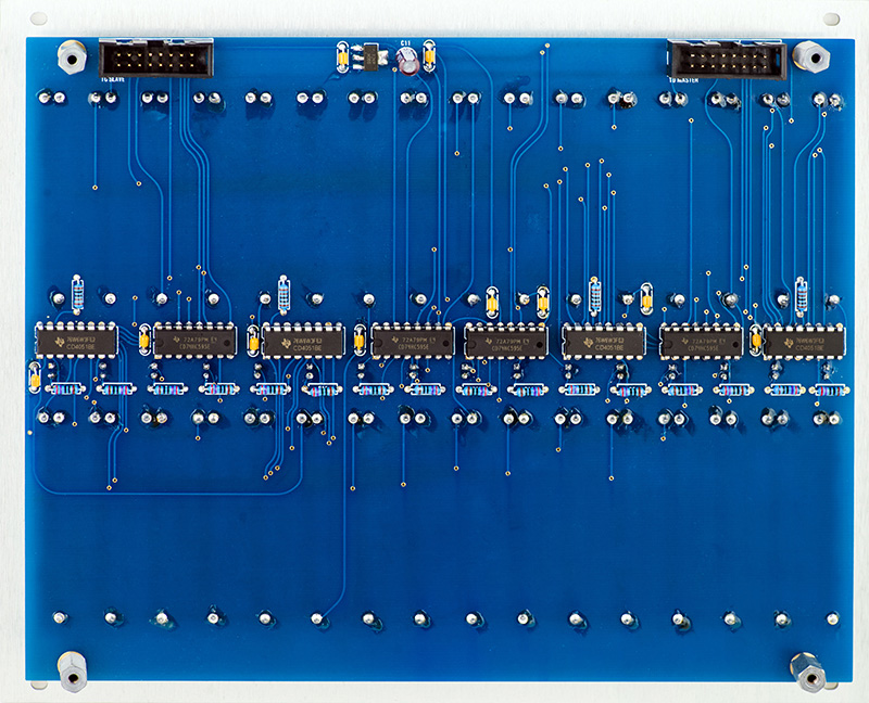
V2 is designed on two PCBs with thru-hole parts. I made reference diagrams from the PCBs.
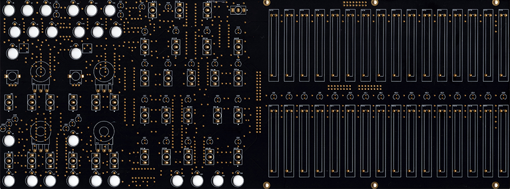
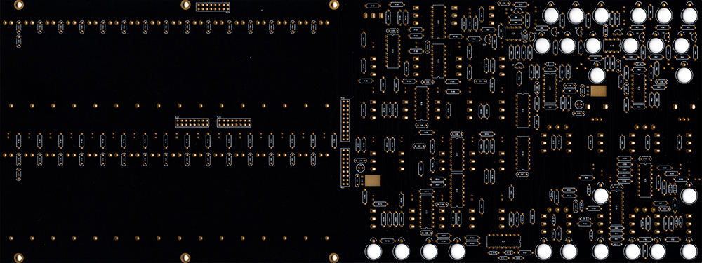
The silk screen reference numbers are way too small and it is hard to tell 3, 6, 8, and 9 apart in some areas on PCB1. I made a higher resolution image of just the component area to refer to when I couldn't read the silks screen.
PCB1 component reference numbers
The BOM has several errors which I corrected.
248 MARF V2 PCB1 BOM Rev 2.0 corrected
248 V2 PCB2 BOM Rev 2.0 corrected
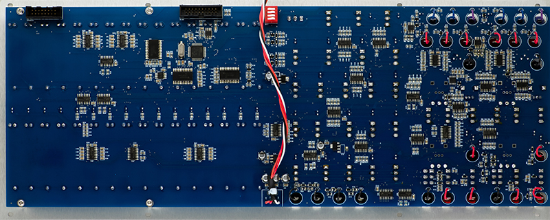
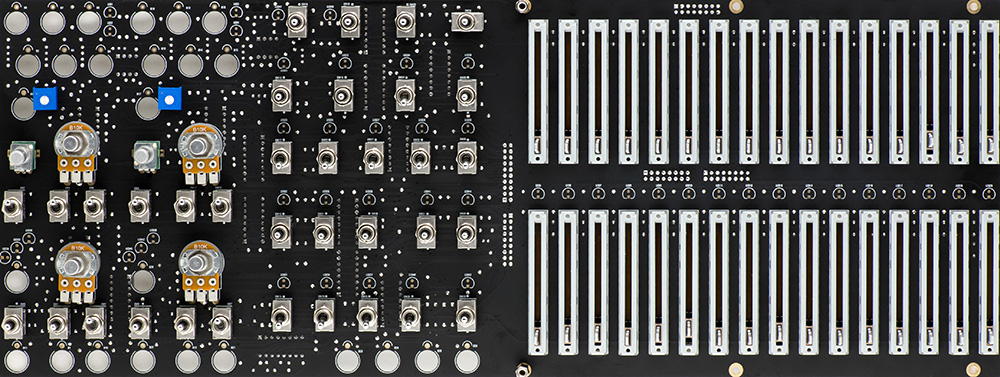
Here is PCB1 assembled without the LEDs installed. I added a 15mm FF and 12mm MF standoff in the mounting holes between the sliders and the circuitry to mount PCB2. There is not a panel hole for the 15mm but it will sit flush against the panel.
The small dots near the switches indicates the momentary side. I installed about 6 switches at a time and then installed the panel and mounted it with two screws and a couple of switch nuts to line up the switches correctly before soldering. It took time but all the switches are correctly aligned.
I have the potentiometers only soldered by one pin until I mount the panel. Once the potentiometer is fastened to the panel I reflow the one pin to relieve any stress. Then I solder the remaining pins. The flatted side of the LED silk screen indicates the cathode side of the LED. I install the LEDs but do not solder them until after the panel is installed. They I can push the LEDs flush with the panel and solder.
I use the female board-to-board connector on the rear of the PCB with the power cable attached. That way if the power cable were connected there are no live male pins on the rear. This is typically the opposite of the BOM.
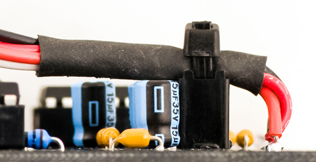
Here is PCB2 with the ST Card installed. The power cable routes towards the PCB and interferes with the electrolytic capacitors (see below). Had I known this before I assembled the PCB I would have installed these three capacitors from the rear at right angles with their leads bend 90 degrees.
There are components under the ST Card on PCB2.
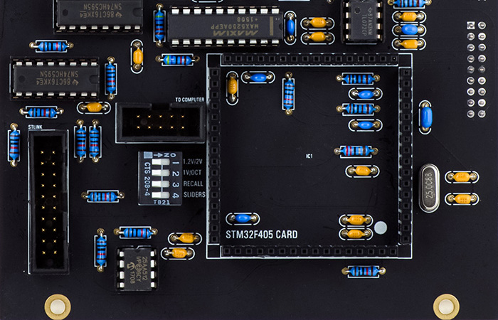
The power cable isn't very well thought out. It routes into the row of electrolytic capacitors so if you tie strap the cable to the PCB it puts stress on the capacitors. The best option is to mount the capacitors on the backside of the PCB. The spacing is close but sufficient for the capacitors in the BOM. I chose to make a standoff to raise the power cable over the capacitors since they were already installed.
Here is the final assembled V2 from the rear.
Programming is straightforward using ST Link. I have instructions for loading ST Link on my 218 page as they use the same STM32F505 processor. However, once programmed, the Time Multiplier and Stage Address controls and the Output Voltage Level sliders did not function. The build thread mentioned bad eeproms affecting the Time Multiplier and Stage Address controls. This doesn't make a lot of sense to me as the eeprom is directly interfaced to the ST32F405 processor and lack of data shouldn't affect reading the controls and sliders. I did buy additional eeproms in two different varieties and neither made any difference as I expected.
I thought I would try reprogramming the firmware. However, once programmed, ST Link could no longer connect to the target. I don't understand why. Typically this would be due to the program redefining the SWDIO, SWCLK or SWO pins, but these pins are only used by the ST Link programmer so it doesn't make sense they would be reprogrammed. The various help files say to use a hardware reset but I could never detect ST Link driving the NRST line going low. I manually pulled it low and that made no difference. Finally I found one hint about pulling BOOT0 high. Boot0 is pin 60 and tied low through a 10K resistor. Vdd is pin 64 so I simply jumper the two while programming but DIP switch 3 must be off. Programming made no difference.
I had verified my build so the last thing on the list was a bad etch. I started a the wiper of the Time Multiplier potentiometers and traced the signals back. That was extremely difficult with these black solder masked PCBs (I don't know why designers use black solder mask other than to make sure their boards are unrepairable and destined for the trash heap). With enough diligence I found open runs on both PCBs. Jumpering them restored normal operation.
CV Jitter
I help individuals by email troubleshoot and repair their modules. I was
helping two individuals with "jitter" on their CV outputs in
continuous mode, but not quantize. I thought it might be related to power supply
noise as the AC-DC and the DC-DC modules are quite noisy. I measured my CV
and was surprised to see "jitter". You can clearly hear it in a
VCO pitch.
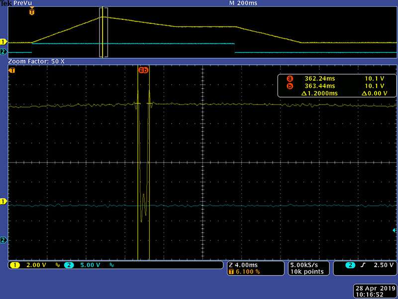
I moved my 248 to my bench with my linear supply and it made no difference. This is a scope image of CV1 on stage 1 when stopped. It shows a lot of high frequency noise but you can clearly see the baseline vary. I estimate the variance at around 25 mV which is 25 cents on a 1V/Oct system.
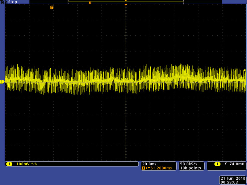
In quantize mode the jitter disappears; the high frequency noise remains. I cannot correlate the jitter to any power supplies or the slider voltage. In fact the jitter is the same with the slider on minimum and maximum. I theorized that noise on the analog input could be minimized by quantization. The analog inputs are multiplexed together so difficult to view. The jitter does reduce when in limited mode but is still present.
The CV outputs use the internal processor DAC converter. The Time output shows similar jitter but uses an external DAC converter. That leads me to believe the issue is either the analog input and conversion or the software.
In quantize mode the jitter disappears; the high frequency noise remains. I cannot correlate the jitter to any power supplies or the slider voltage. In fact the jitter is the same with the slider on minimum and maximum. I theorized that noise on the analog input could be minimized by quantization. The analog inputs are multiplexed so difficult to view.
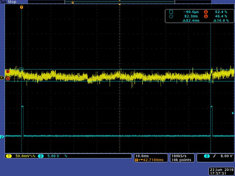
This scope image shows a 2 stage cycle. I added a 0.01 µF capacitor on the output and with the 220R series resistors forms a low pass filter with a cutoff about 70 KHz. This adds minimal skew to the output. The pulses indicate the time for a single stage. Note the high frequency noise has been significantly reduced. This image indicates about 40 mV of jitter. This image also verifies the jitter is present when running similar to when stopped.
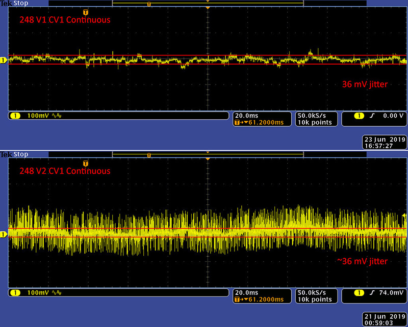
I was fortunate to have a 248 V1 come in for repair. I measured the CV output with the exact same setup and found it exhibited about 36 mV of jitter. This scope image composite shows the jitter in a V1 and V2. Note V2 does not have the output capacitors which reduce the amount of high frequency noise. I added the red lines to roughly measure the jitter on V1 and then transposed those same lines and spacing to V2. My conclusion is that both V1 and V2 exhibit jitter. V2 exhibits more high frequency noise. The jitter is not related to power supplies and my conclusion is it is likely due to the software.
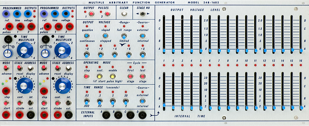
Operation
The MARF is quite complex. Here I have a simple ADSR patch programmed. The gate is short but I have the S sustain until the gate goes false.
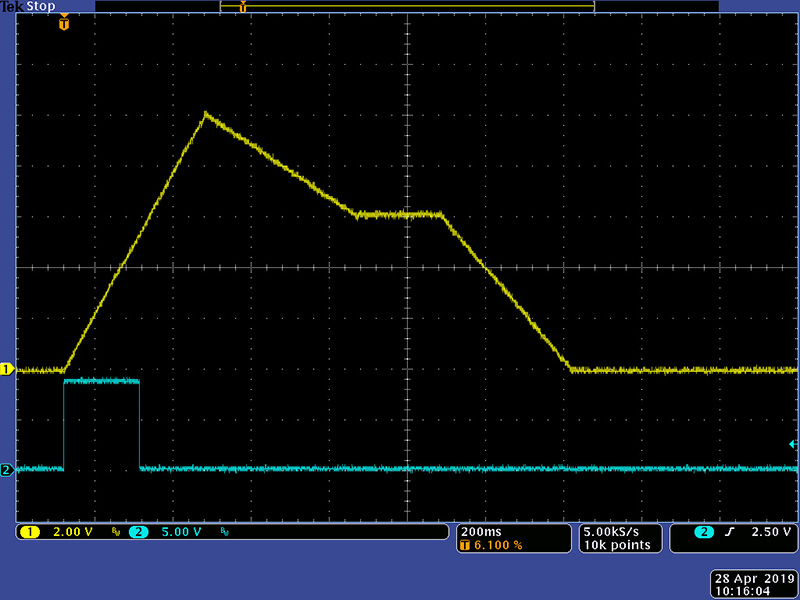
Here's another with a visible glitch.

The glitch is 1.2 mS. Digital systems should be able to output continuous waveforms without transition glitches but it is short so likely is unnoticeable.
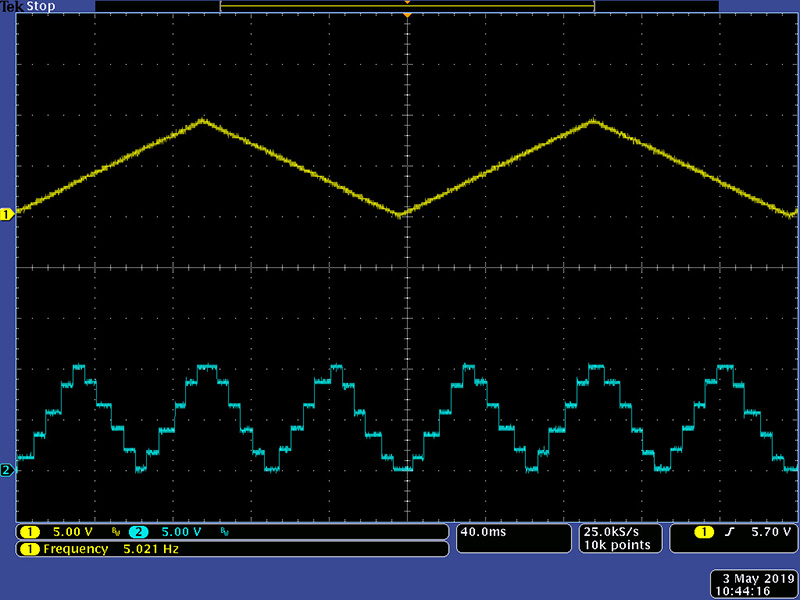
Here I have the 248 setup for external addressing with a triangle wave. I used my DJB-004 module to have the triangle be precisely 0 to 10V. I have the sliders setup for a frequency tripler. Note that in external addressing sloped is not available since the time per segment is undefined. It works pretty well at 5 Hz. There is some variation in pulse width due to synchronization with the processor sampling.
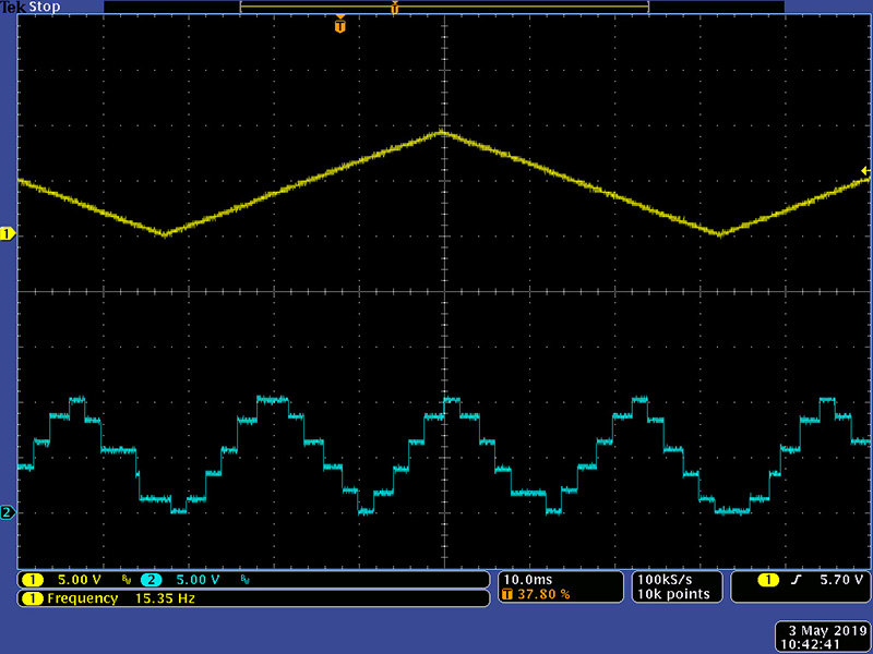
At 15 Hz the performance is still pretty good.
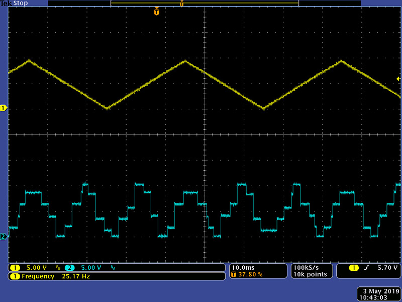
Above 15 Hz the processor begins to miss samples as shown in this 25 Hz waveform and can be seen in the stage LEDs.
Epilog
I had a 248 that Start2 operated strangely. It would always reset to stage 1. Upon investigation, Strobe2 wasn't connected to PLD1 pin 12. I suspect Start2 caused crosstalk with Strobe2 which is on the next pin and so would reset to stage 1. I assumed this was an easy fix and looked for where to jumper the run but I couldn't find one going to PLD1 pin 12. I added a wire but it turned out that Strobe 2 was shorted to Strobe 1 after the input 4K7 resistor. I found a trace between the anodes of D7 and D20 which are the over voltage protection diodes for these signals. I cut this trace but the signals were still shorted together. Since the unit was built, I couldn't inspect the front, and with this crappy black solder mask it's nearly impossible to trace the runs anyways. I ended up lifting R74, R78 and D7 and wiring it all above board. This is just another example of the lack of quality that went into these designs and documentation.
Expander
Expander modifications to operate with V2 are located on the V2 modifications page.
I did not build this 248 Expansion but needed to verify it with the 248 V2 MARF. The sliders on the Expansion are powered from a reference supply through pin 9 on the expansion cable. This pin is unconnected on PCB2 so the Expansion sliders are unpowered. On V1 this reference supply is 5V and on V2 it is 3.3V. The logic on V2 PCB2 is also 3.3V so I jumpered IC31 pin 16 to To Slider IDC connector pin 9.
I was never able to get the V1 Expander working with the V2 MARF. The Voltage Level sliders worked correctly but the Interval Time sliders corrupted all analog data. The processor reads the 68 analog controls using a series of 74HC595 shift registers which address CD4051 analog multiplexers. The last 74HC595 in the chain always has its last output, pin 7, low which enables the CD4051 to always have its data on the analog bus. If the sliders are lowered then it puts 0V on the bus through a 1K series resistor which attenuates the analog data by half. In addition, Time Interval sliders 17 and 25 seem to put their data on the analog bus at the wrong time, thus also corrupting the data. This serial data stream is asynchronous to the sequencer operation and has a lot of jitter which I suspect are delays caused by interrupts. Since there is a missing power run, a V1 Expander was never verified to work with a V2 MARF. I returned the unit to the customer with the belief that the firmware has issues.
Update1
After I returned the module to the customer I found this on the
ElectricMusicStore V1 Expander Order page. "This is an expander for the 248 Rev.1 (MARF Rev.1 SMT version).
It is not working with the current firmware on the MARF Rev. 2 (thru-hole version). We are working to get it fixed ASAP."
Even with the new firmware you will need to connect IC31 pin 16
to To Slider IDC connector pin 9 on the V2 PCB2. Also note that if you have
programmed V2 with 2.0, you cannot reprogram it with new firmware without
pulling Boot0 high by jumpering the STM32F405 pin 64 to pin 60 and setting DIP
switch 3 off during
programming.
Update2
Expander modifications to operate with V2
are located on the V2 modifications page.