|
V2 Modifications |
|
There are a number of issues with V2. A team of talented individuals have invested a lot of time investigating and updating the software and hardware to address these issues. The goal has been to keep hardware modifications to a minimum to be able to retrofit existing V2 boards. There are two versions of the boards - ElectricMusicStore and SAModular which have some differences which will be noted. [Edit - I believe now the latest SAModular boards incorporate all/nearly all of these modifications.]
Numerous bugs have been addressed - see the Software section at the bottom for details. Two major usability issues addressed were CV "jitter" and the non-functional Expander.
Note that with default software, you need to pull Boot0, pin 60 on the processor, to 3.3V and set DIP switch 3 to off in order to reprogram it. Pin 64 is 3.3V so you can jumper pin 60 to pin 64 during programming.
These are the modifications I made to my 248 and Expander. I describe each as essential or improvement to performance or functionality. I believe them to be correct but offer no warranty or guarantee nor accept any liability for any issues that may arise from these modifications.
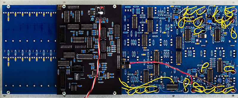
248 V2
CV Output Jitter
The sliders are all read by a single ADC input on the processor. The signals are multiplexed by CD4051s and there is considerable noise in the system that causes a wide variation in converted values. Three main efforts have been utilized to minimize this variation.
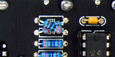
The CD4051s used to multiplex the signals have been replaced with MAX4617s. These are pin compatible devices with a smaller over voltage spec (see Over/Under Voltage Protection section below). Replace IC24 on PCB1 and IC22, IC23, IC27, IC28 on PCB2. This modification improves performance but is not essential.
The software has improved filtering on the analog slider values.
A new processor daughter board moves critical components from PCB2 to as close as possible.
The software alone offers a great improvement in reducing jitter. The hardware modifications offer further improvements but are not essential.
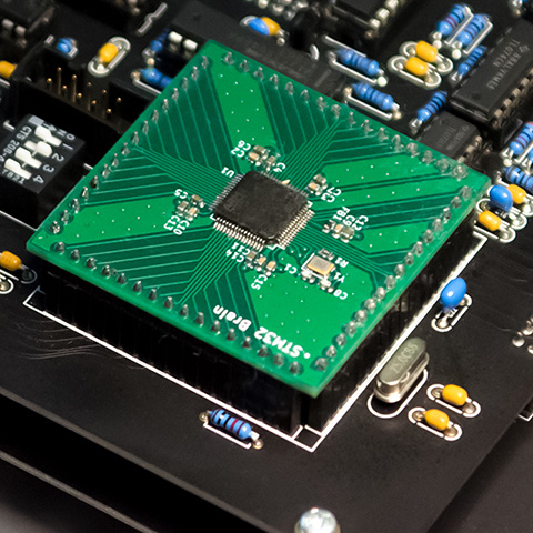
No plans have been made regarding this new processor daughter board but SAModular does sell a replacement PCB2 for the ElectricMusicStore 248 V2 to eliminate the daughter board and associated long traces by incorporating the processor and critical components on the PCB.
SAModular has redesigned their 248 V2.3 and later PCBs in a similar fashion.
Other areas including improved power and ground routing and analog filtering have been investigated but have not shown significant improvements.
CV Output Offset
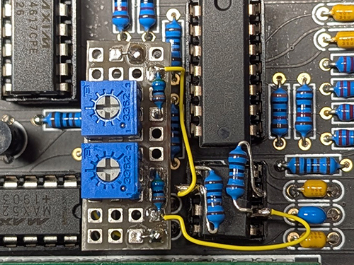
There is no offset adjustment for the CV outputs so they have some positive or negative voltage with the sliders at minimum. This modification adds an offset trimmer for CV output. After implementing the modification let the module warm up, set the offset (mine set to +0.18 mV) and then check the scale trimmer. This modification improves performance but is not essential. Offset without the modification may be positive or negative in the tens of millivolts.
The CV outputs have adjustable gain (scale) and are non-inverting. This modification changes the ground reference to an adjustable reference. The trimmer needs +/-15V which is not easily accessible so I simply soldered the trimmers to the tops of the ICs. The modification consists of lifting a resistor, and adding two resistors and a trimmer for each CV output.
Some users report having to change the 100K to 49K9 in order to achieve zero offset.
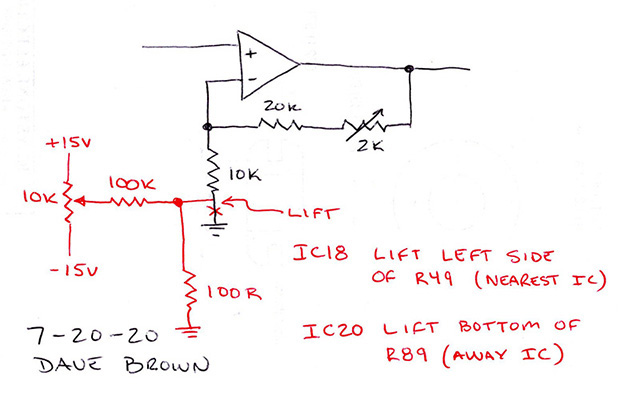
IC18 is used for CV 1
IC20 is used for CV 2.
Over/Under Voltage Protection
There are 20 diodes on PCB1. Most are used as over-voltage protection by clamping various signals to 3.3V. The 1N457 diodes have a voltage drop around 0.55V which clamp the signals at 3.85V. The over voltage specification for the CD4051 is Vcc+0.5V. The over voltage specification for the MAX4617 and the processor is Vcc+0.3V. These parts contain internal clamping diodes and while with series current limiting resistors they will not be damaged, exceeding this specification can result in odd behavior.
An example is using the Time Multiplier CV with the control. When the voltage is clamped to 3.85V, the Stage Address control is affected and advances to the next stage. The solution is to use Schottky diodes such as the SD103B in place of all the 1N457 diodes. This limits the over voltage to within specifications. This modification improves functionality but is not essential. Over voltage can be avoided by keeping the CV input to 10V or less and not adding in more control to exceed a 10V summation.
Slider Minimum and Maximum Values
The processor and Expander sliders are powered by one LT1117-3.3 regulator and the main sliders are powered by a second LT1117-3.3 regulator. The specification over temperature for these regulators is 3.235 V to 3.365 V, a difference of 130 mV. A 10 mA load at 25°C reduces the tolerance to 66 mA. The main regulator load is over 100 mA so a typical difference at 25°C could be 80 mV.
If the slider regulator is less than the ADC regulator the sliders will not reach maximum value. With voltage drops across traces and connectors it is also possible sliders may not reach minimum value. This modification removes IC4 and powers the sliders from the same 3.3V supply as the processor. In addition, a small dead zone in the firmware at each end of the sliders improves achieving minimum and maximum values. Since the sliders only operate over 90% of their travel, this additional dead zone is insignificant.
IC4 must be removed and the POT7 pad nearest to PLD1 can be wired to the bottom of R168. This modification only improves reaching maximum values if the PCB1 regulator is significantly lower than the PCB2 regulator.
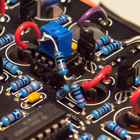
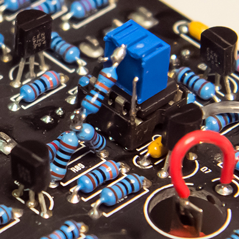
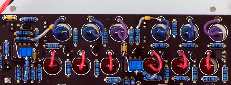
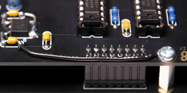
The regulators on my 248 differed by 25 mV with a couple of mV of ground difference. I chose to remove IC4 and hard wire the sliders to PCB2 to eliminate any voltage drop between the PCBs. I was able to achieve equal 3.3V and a 2.2 mV difference in ground between the processor, sliders, and the Expander sliders. You can easily burn out a slider by miswiring power. I added a dot of red and black paint to mark the correct pins in case I need to make repairs. This photo shows my direct slider wiring and you can also see my heavier power runs from that previous investigation.
CV Out Filtering
There is a lot of high frequency noise components on the CV outputs. This noise is fast enough it doesn't really impact operation. There is a 220R series resistor so I simply added 0.1 µF capacitor from the banana jacks to a nearby ground. This rolls off the high frequency components at 7 KHz with a time constant of 22 µS. This modification improves performance but is not essential. In this photo you can also see my offset trimmer modification.
Start / Stop Impedance and Levels
The software has been enhanced to enable external clocking by simultaneous driving both the Start and Stop input jacks. The input impedance of each is 6.9K through a diode. The Start and Stop inputs are attenuated digital inputs to the processor with a Vil is <0.95V and Vih is >1.79V. Ignoring resistor tolerance this requires a low signal at the banana jack to be < 3.4V and a high signal needs to be > 6.0V. Between 3.4V and 6.0V is not allowed/undefined. An issue arises with combination trigger/gate pulses. A 15/7.5V trigger/gate is seen as a single high input but a 10/5V pulse is seen as a high with the gate in the not allowed region.
The driving module with a 10V pulse to both jacks needs to have an output impedance less than 2K2. If it is driving all four inputs then it needs to be less than 1K. Remember patching to other modules will reduce this even further.
The Start and Stop attenuation resistors are low in value. I changed them all to 49K9 which raises the input impedance to 100K and attenuates the input voltage by half after a diode drop. A 5V gate is now a valid high signal. With my Schottky diodes, voltages over 7.5V will clamp to the 3.3V supply and at 15V only result in 222 µA of clamp current. I changed R61, R69, R101 and R109 from 4K7 to 49K9 and R63, R72, R103, and R112 from 2K2 to 49K9. This modification improves performance but is not essential.
Some modules, like the 245, can have the pulse outputs paralleled. Adjacent stages have a continuous gate with multiple trigger pulses. There are two ways to use paralleled pulse outputs to externally clock the 248.
My 245 trigger amplitude is 14.3V and the gate amplitude is 6.7V. Both are a valid high for the 248. Interconnecting the 245 and 248 with a 100K series resistor provides sufficient attenuation to generate a valid high and low level. Note that modules with different trigger and gate voltages may require a different value resistor.

Zooming in on the center pulse we can measure the amplitudes. The 14.4 trigger is attenuated to 4.4V and the 6.7V gate is attenuated to 2.4V. This generates a valid processor Vih of 2.05V and a Vil just a bit above the specification but within the margin of the processor at 1.05V. Note that modules with different trigger and gate voltages may require a different value resistor.
You can also capacitively interconnect the modules with a 2N2 capacitor. There is no impedance to discharge the capacitor it needs a parallel 4M7 resistor. You can see the RC decay of the 245 pulse.
Zooming in on the center pulse we can measure the amplitude. The 14.4 trigger is attenuated to 7V and the 6.7V gate is effectively blocked by the capacitor for a valid Vih and Vil to the processor. Note that this method should work with any module trigger and gate levels.
Panel
The panel on the 248 is floating and can pick up and radiate noise. While a properly grounded boat will ground the panel, I wanted it connected when on the bench so I added a wire from the ground on a capacitor to a standoff pad. You have to use a standoff which screws to the panel. You can also see my heavier power runs in this photo. This modification is not essential.
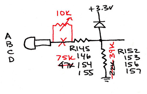
ABCD Input Impedance
The ABCD inputs are attenuated with a 47K/22K network with an input impedance of 69K. When you parallel all four to do calibration, the input impedance is 17K25. If you are generating the 10V reference with a module, the output impedance of that module will reduce this voltage resulting in an inaccurate calibration. For example if the source module provides 10V with a 1K output impedance the voltage on the ABCD inputs is only 9.45V. The 248 is best calibrated using a 10V power supply.
Time Multiplier Controls
The BOM specifies 10K - 100K for these controls. This isn't quite right. These potentiometers are voltage attenuators driving a 100K circuit. As such, the 100K input impedance affects the attenuation. If these controls are 10K then the front panel legends reasonably are accurate. If these controls are 100K, then the taper is more log and 1 is closer to 1.4 and 2 is closer to 2.3. The linearity of the Stage Address is also affected similarly. You should use 10K for these four controls.
DIP Switches
DIP switch 3 was used to not save / save slider information. The software saves slider information but moving a slider overrides the saved position so this function is no longer needed. DIP switch 3 should be set to OFF to enable programming.
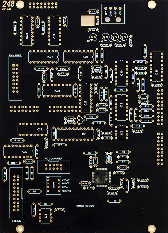
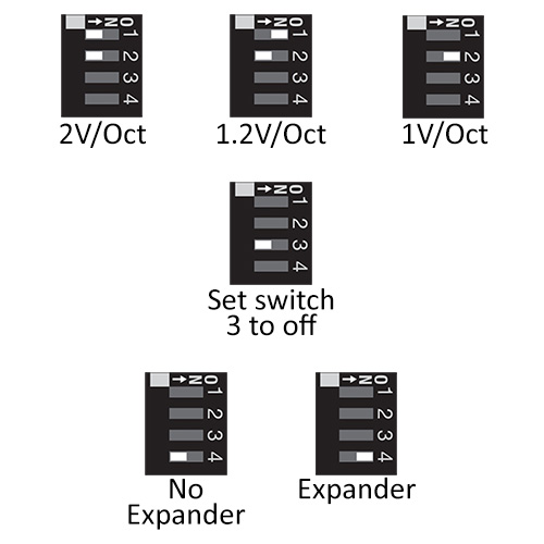
The V/Oct DIP switch positions in the V2 manual are wrong. This illustration shows the correct DIP switch settings for V2.5 software.
Epilog Sept 12, 2025
I modified a customer's 248 with all of the preceding modifications and the V2.66 firmware. Their feedback was positive with the exception of the ABCD external inputs. Those voltages routed to the AFG CV were quite a bit lower. I then went and checked mine which was even worse. The external inputs are attenuated to a range of somewhere between 0.313 to 0.325. The ideal is 0.330 to drop a 10V input down to the 3.3V processor level. A delta of 17 mV is expanded to 51 mV but I was seeing more than that variation between channels.
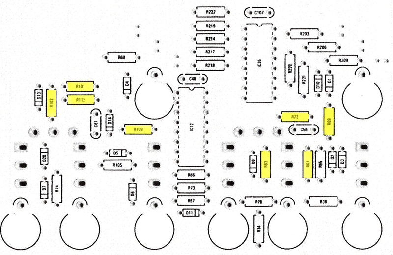
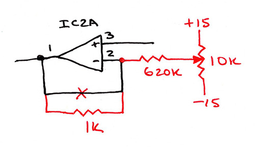
I decided to make two more modifications. IC2A on PCB2 is used as a voltage follower to buffer the multiplexer for the potentiometer and external inputs. The op-amp will have offset and will impact the voltage accuracy. I added an offset control for each which just very slightly changes the gain. I lifted pin 2 and pin 6 and added the 1K resistors on the IC. I had to make a small daughter board for the two trimmers. I chose 1/8W resistors and used 560K since that is what I had in stock. The daughter board is held in place with solid wires down to +15V and -15V at decoupling capacitor pins.
Calibration: Power on the 248. Turn full CCW the four main potentiometers and center the two attenuverters. Leave the external inputs ABCD unconnected. Connect a DMM to PCB2 IC2 pin 1 and adjust the trimmer close to 0V.
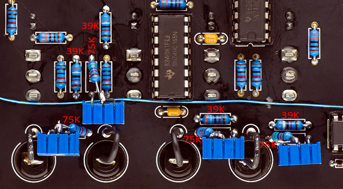
I replaced the fixed resistor attenuators for the external inputs to increase the impedance and add a trimmer. I chose a 10K trimmer wired such that the adjustments all face to the bottom of the panel. I lifted one end of R145, R146, R154, and R157, soldered one end of the trimmer to the PCB and the wiper to the other end and the lifted resistor lead.
Change R152, R153, R156, and R157 from
22K to 39K 1%.
Change R145, R146, R154, and R157 from
47K to 75K 1% in series with a 10K trimmer. I used 1/2" square trimmers as the
leads were longer.
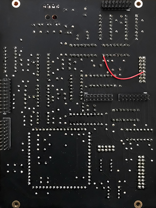
Ignore the blue wire as my PCB had a short that I ended up bypassing.
Initial calibration: Center all four trimmers. Power on the 248 and apply 10V to each input individually and adjust that trimmer for 3.30V on either the junction between each pair of resistors (R152-R145 etc.) or on IC24 on PCB1. A is pin 13, B is pin 14, C is pin 15, and D is pin 12. Calibrate the 248 per the standard procedure.
Final calibration: It is important to set the CV output offset first, then the scale. I found a better way to scale is to have no CV input and adjust the scale so that the +2 to +8 limit switches read as close to the V/Oct multiple as possible. I adjusted mine so that +4 to +8 were exact. +2 was a bit off. Then connect your volt meter between the AFG CV output and the external input. I used AFG1 Stage1. Set stage 1 to external. Apply any fixed voltage (I used 5V) to Ext A, set switch to external and the slider to A. Adjust the trimmer to get as close to a 0 reading as possible. Repeat for inputs B-D with the sliders set at B-D. I verified with several different input voltages.
When calibrating this way, my sliders no longer reach 10V, but are 36 mV shy at 9.964V. However, the limit switches are accurate to within a few mV.
Expander
The Expander requires updated software to function. However, a modification might be required on the 248 PCB2 to supply 3.3V to the Expander ribbon cable connector. Pin 9 on the "To Sliders" IDE connector should be 3.3V. The square pad is pin 1 and that row are the odd numbers, so pin 9 is the 5th pad. 3.3V can be found on pin 16 of IC23 or IC31 (the photo shows IC31). You do not want to power the Expander sliders from the Expander 3.3V regulator as that adds another regulator with tolerance. This modification is required to operate the Expander with ElectricMusicStore boards and SAModular boards prior to V2.3s. SAModular V2.3s and higher include this missing trace.
V1 Expanders use a LM1117-5.0 regulator. V2 Expanders should operate on 3.3V so IC9 should be a LM1117-3.3. Expanders are likely to work without this modification but are driving 5V logic with 3.3V signals. Similar to the 248, replace the CD4051s on the Expander with MAX4617s. Replace IC1, IC2, IC6, and IC7. The BOM calls out 270R resistors. I chose to build mine with 330R although either will work fine.
This is the updated BOM with changes that I used for my V2 Expander.
Software Updates
Software V2.66 Sept 5, 2022
Max Lord has continued to work on improving the software and has rewritten a considerable portion. A main goal is to emulate the original 248 as closely as possible. V2.66 has now been released and is available. Details are on Modwiggler MARF 248 New Firmware Announcement. The release notes are also on Github but are also available here. This is my summary of the changes.
V2.66 changes:
Programmed pulses fire correctly in all modes, whenever a step changes.
Reference signal present in all modes, whenever a step changes.
Steps set to sloped mode will now slew correctly in all modes including advance, strobe and continuous address.
Quantize mode works correctly on full range steps.
Loop behavior is correct. Loops now search backwards from a "last" step to the closest "first" step. Multiple loops are now possible.
The "level 2" programming is organized into a single bank. It is no longer different between AFG1 and AFG2.
External inputs no longer have audible slewing.
Glitches in voltage output fixed.
Step times match panel legend exactly.
AFG Section Shift:
AFG1 and AFG2 now both access the same memory. If you do not have an Expander,
then you can use section shift for more flexibility.
Press Stage Address Display 1 + Stage No Right to move AFG1 to steps [16-32].
Press Stage Address Display 1 + Stage No Left to move AFG1 back to steps [1-16].
Press Stage Address Display 2 + Stage No Right to move AFG2 to steps [16-32].
Press Stage Address Display 2 + Stage No Left to move AFG2 back to steps [1-16].
Save and Load Program:
This version supports saving and loading 16 programs.
Saving programs:
Press the Clear switch down briefly to save the current program.
The Marf will stop running if it is running.
The Pulse LEDs will toggle indicating that you are in the Save mode.
Press either of the Pulse switches in either direction to abort the saving mode.
Use the Stage No switch to select one of the 16 memory locations. The step LED will indicate the selected program number.
Press the Clear switch down again briefly to save the program. The LEDs will flash in a downwards pattern indicating that the program was saved.
You can continue with whatever you were doing.
Loading programs:
Press the Clear switch up briefly to load one of the saved programs.
The Marf will stop running if it is running.
The Pulse LEDs will toggle indicating that you are in the Load mode.
Press either of the Pulse switches in either direction to abort the loading mode.
Use the Stage No switch to select one of the 16 memory locations. The step LED will indicate the selected program number.
Press the Clear switch up again briefly to load the program. The LEDs will flash in an upwards pattern indicating that the program was loaded.
All of the sliders will now be “pinned” to their saved values. To restore a particular slider’s activity, the slider must be moved through the saved value, at which point it will begin operating normally again. If you aren’t sure, move the slider to 0% and 100% and then back to where you want it. This is similar to how the 200e controls behave when restored.
Input Pulse Operation:
A simultaneous pulse to start and stop is the same as the manual advance switch.
A simultaneous pulse to strobe and start will correctly start on the strobed step.
This release required significant refactoring to almost 100% of the code base, including all of the core function generation logic, all of the interface code, and much of the internal scheduling logic. This release is able to run at 8x the timing resolution of the previous version.
Internal performance, operational and code health improvements:
Using a much better filtering algorithm consistently on all ADC inputs. Fixes slewing on large jumps and jitter on steady state signals.
Output sample rate increased from 4kHz to 32kHz.
Voltage quantization and timing computations use higher precision floating point calculations.
Numerous bugs with start/stop and sustain/enable modes ironed out.
Slow code moved out of IRQs into main loop and scheduling tightened up.
Inlining small methods and compiling with speed optimizations.
Reduced function call overhead in peripheral drivers.
Improved display update system lights LEDs better when the clock is at high speeds.
Applied consistent code style guide including capitilization, indentation.
Improved naming conventions using more standard terminology.
The option to reverse the pulse LEDs has been moved to the calibration routine.
Calibration Procedure:
Hold Stage Address 1 Advance down during power on.
LEDs now are cycling.
Turn all controls to maximum, and apply 10v (as measured on the banana jacks) to all 4 external inputs.
Select pulse 2 up if you need to swap the pulse LEDs. LED will move to pulse 2.
Select pulse 1 up to swap it back to normal.
Press Stage Address 2 Advance down to save calibration.
It will ERASE the entire memory, including saved programs.
Previous Releases
Version V2.5b3 is available on the Muffwiggler thread MARF 248r source code available and may still be at SAModular under the Firmware tab.
V2.5b3 changes:
External input for Stage Address 2 now calibrates.
1st stage after Enabled stage causing a stop now sends a Programmed Pulse.
1st stage after Sustained stage causing a stop now sends a Programmed Pulse.
Programmed Pulse timing on stages selected by External Stage Address input corrected.
Interval Time slider settings are now recalled with preset.
Improved quantization.
Updated slider value filter to reduce amount of CV jitter.
After loading a preset, moving a slider will activate that slider with correct values.
DIP switch 3 is disabled to allow the debugger to connect and program without having to pull Boot0 pin 60 high.
The Expander does not function with this version.
DIP switch 3 was used to not save / save slider information. The software saves slider information but moving a slider overrides the saved position so this function is no longer needed. Leave in the off position.
Version V2.5 is available on the Muffwiggler thread MARF 248r source code available
V2.5 changes:
Expander functionality - elimination of slider data corruption, correct slider 17 operation, improvements to slider, switch, and LED serial timing, and improvements for more consistent minimum and maximum slider values.
Sliders (when calibrated properly with offset and scale) should reach full voltage range (all 32 of my sliders read 0.00V to 10.00V).
Reduce skew for Stage Address control and external CV.
Improve Advance switch operation.
Fixed AFG1 Cont/Strobe operation.
Enhancement: Output pulse LED swap option.
Enhancement: External clock.
Enhancement: Swing mode with external clock.
DIP switch 3 is unused. Leave in the off position.
V2.5 Enhancements This two page document describes the new enhancements and can be appended to the V2.0 manual.
Output Pulse LED Enhancement: The Output Pulse LEDs are swapped. The hardware fix is a simple modification to cross resistors R219 and R222.
The software addresses this issue but to be compatible with boards built with and
without these resistors crossed, a power-up sequence saves the correct
configuration in eeprom.
Power on the 248 while holding both Output Pulse 1 and 2 switches in the off/down position.
Output Pulse LED 1 will start to blink but this could be either LED based on whether the above modification has been done.
If Output Pulse LED 1 is blinking (resistors crossed) then press Output Pulse switch 1 to the on/up position to save this configuration.
If instead Output Pulse LED 2 is blinking (resistors not crossed) then press Output Pulse switch 2 to the on/up position. This will save the configuration to reverse these LEDs in software.
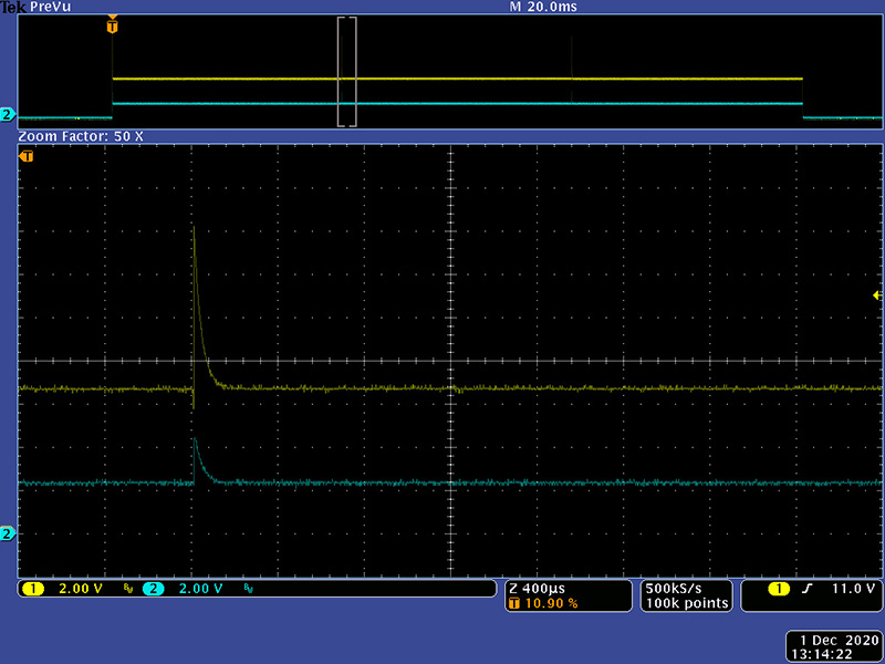
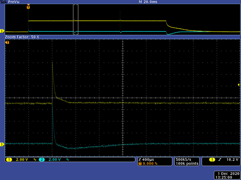
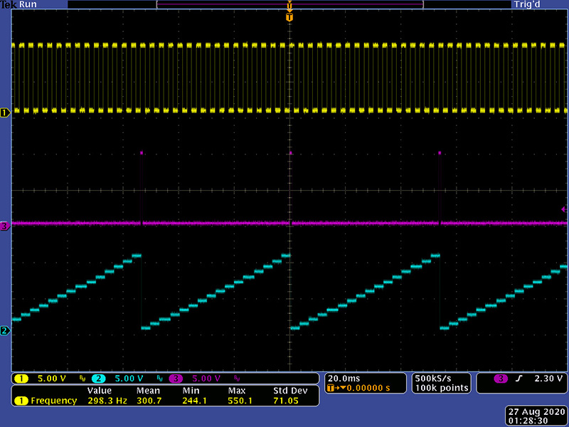
External Clocking Enhancement: External clocking is now enabled by driving both the Start and Stop jacks together. Advance will clock to the next stage. This photo shows the 248 driven by an external 300 Hz clock.
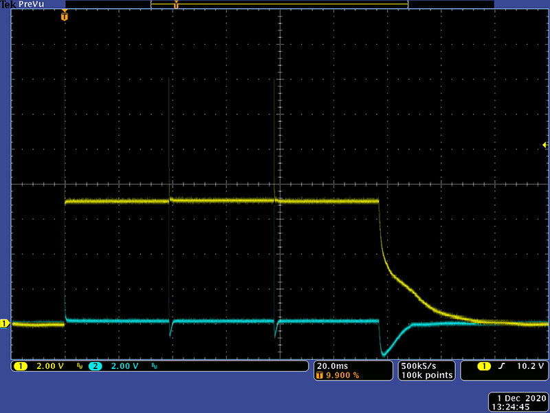
External Clock Swing Mode Enhancement: When driving the 248 with an external clock, the Time Range switches, Time Multiplier, and Interval Time sliders have no function. The Cont / Strobe switch is repurposed as a Swing Mode enable/disable switch. Pressing it down momentarily while externally clocking enables Swing Mode and pressing it up momentarily disables Swing Mode. Note this is a global, not a per stage, mode.
When enabled, it will cause a second pulse to be output on the All Pulses jack. The time between pulses is controlled by the Time Range switches, Time Multiplier, and Interval Time sliders. If you want to "disable" swing mode on a particular stage, set the Time Range switch to 0.002 and the Interval Time slider to minimum for this stage. There are still two pulses but they are now very close together.
Modified 248s
I was sent a 248 V2 which was a prototype with a few differences. I built and installed the SAModular EMS PCB2. The yellow wire connecting with a separate connector to V2 was a missing run on the prototype. The offset modifications can be seen by the blue trimmers added on top of the ICs. This version used the zener diode overvoltage protection as on V1 which does not include undervoltage (e.g. negative) protection so I replaced them all with Schottky diodes. The blue wires are all the added Schottky diodes to +3.3V.
What was odd is the attenuation resistors for Strobe1 were connected to Strobe2 and there was no connection to Strobe2 on PCB2. There must be runs connecting parts together on the front of PCB1 so I had to add all the Strobe2 parts above the PCB. I removed the pins from PCB2 so there was no connection to PCB1 and ran the brown/red wires to another connector on PCB2.
What is strange is my black/gold V2 had this exact same issue and required the same modification. I know there are V2 versions that don't have this issue so I can only conclude there are undocumented multiple versions.
The good news is the V2 EMS PCB2 from SAModular works great.