|
Moon Modular M569 Quad Sequential |
|
While I like thM569 sequencer a lot, I really want to be able to slave other devices to it. You can use the Shift inputs to drive the M569 from an external clock but it would be nice to have the Clock and Run signals to control other modules. There is a separate PCB for the clock generation circuitry with a 14 pin interface. I mapped out the pins and and designed a companion module to buffer these signals.
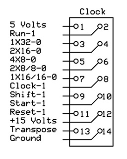
Connector top view - key to left
A new clock interconnect cable brings these three signals and ground out to a MTA connector.
Besides the buffered M569 Clock, Run, and Reset signals I wanted a Moog-style Start and Stop circuit to gate an external clock to drive the M569 Shift input. I designed a Start/Stop flip-flop with debounced switch and input jacks to gate an external clock. The design ensures there are no truncated clocks or glitches.
M569 Companion Schematic Updated
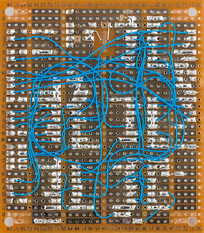
I built the circuit on a small perfboard with the power and ground runs on the top. In this photo I did not yet have the 74HC86. Power consumption is +5V at 10 mA.
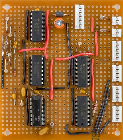
There wasn't a lot of wiring so the board build went fast. I did make modifications after this photo was taken.
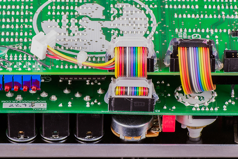
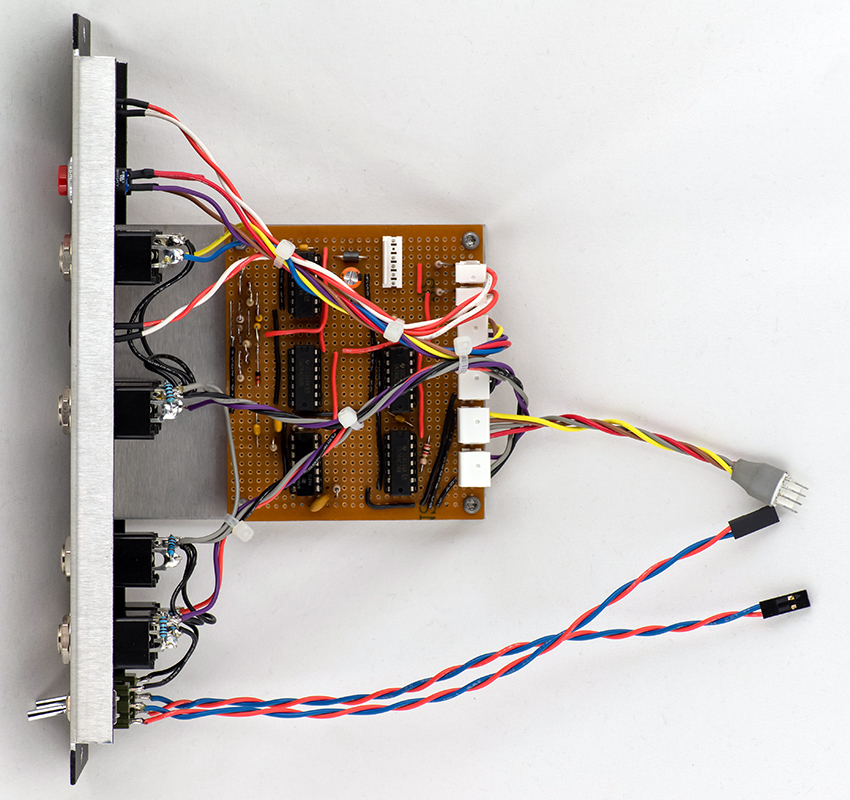
The four conductor MTA header connects to the new ribbon cable on the M569. I used epoxy to seal the pins after soldering and then added heat shrink. The two twisted pair cables have FCI connectors to mate with the square pins for the row 3 and 4 transpose modification on the M569.
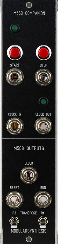
My 1MU panel has the external clock control on the upper half and the buffered M569 signals and transpose switches on the lower half. The Clock In is normalled to the M569 Clock Output.
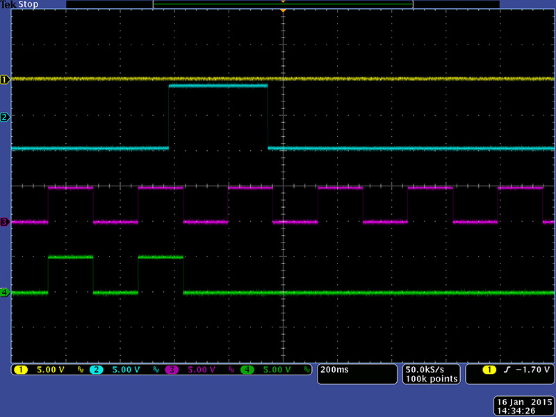
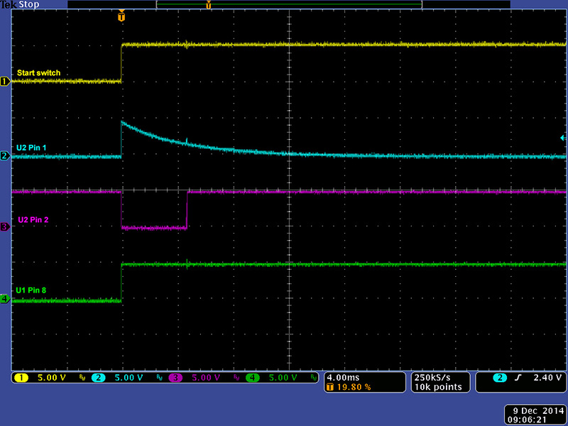
I use a simple differentiator into a Schmitt trigger gate to debounce the switches. This image shows the start switch, differentiator output, Schmitt output pulse and the flip-flop run signals.
I needed to ensure there were no glitches on the Clock Out signal for any modules downstream that are edge sensitive. The critical transitions are when the gate (e.g. sampled run signal) goes false as the clock goes true, and when the gate goes true as the clock goes false (the other two transitions are don't care). My solution was to delay the clock to the flip flop by 1 uS which delays the gate by 1 uS and adding a 10 uS delay to only the rising edge of the clock. Thus when the gate goes false the clock doesn't go true for 10 uS and gate goes true 1 uS after the clock goes false. I used the two extra XOR gates in the in the flip flop clock path since I would have had to tie the inputs to a logic 0 or 1 anyways.
![]()
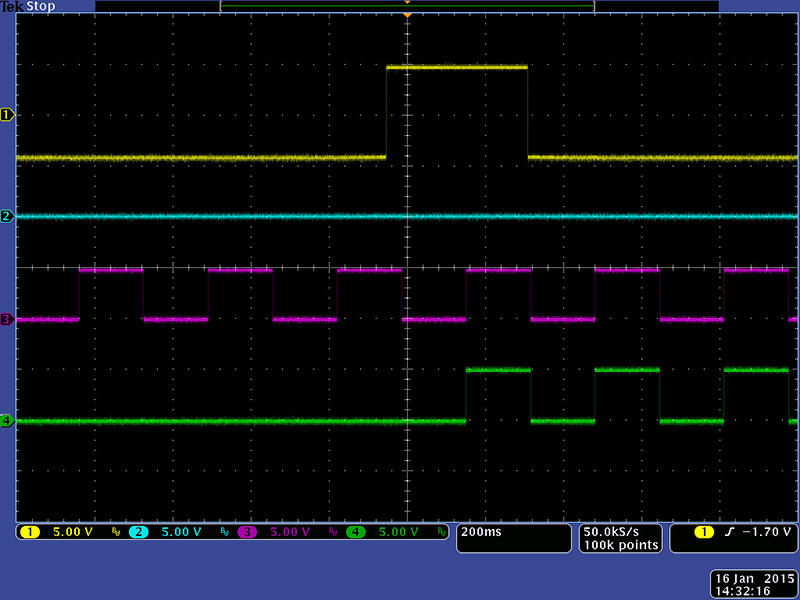
This scope image shows a Start pulse while Clock In is high so Clock Out doesn't start until the next cycle when Clock In goes high. I have under and over voltage protection on the inputs as the Start and Stop pulse are +/-5V signals.
This image shows a Stop pulse while Clock In is high so Clock Out completes a full cycle and stops when Clock In goes low.