|
277M Signal
Delay Unit |
|
The modern clone 277 modules are built using digital signal processors. The 277, designed in 1972, was likely one of the first digital delay units. It uses 48 1024 bit shift registers to provide a delay from 50 mS to 200 mS as indicated by the panel legends.
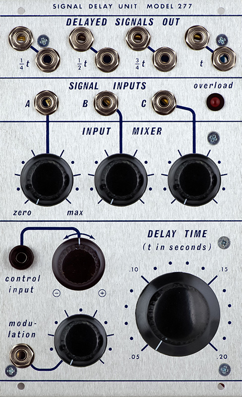
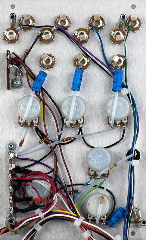
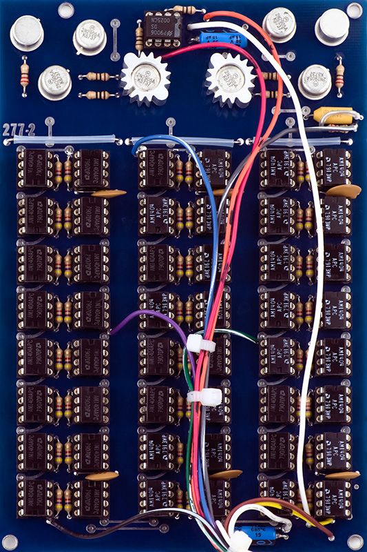
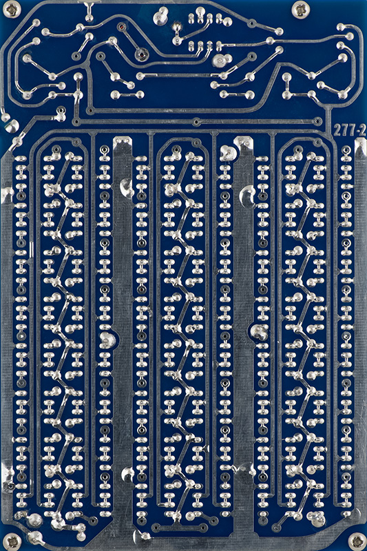
The design is two PCBs with front panel wiring.
The schematics for the 277 are in very poor condition and portions are literally unreadable. They also contain errors. In bringing up this module I had to make some assumptions and modify portions of the circuitry for some basic functionality. Only one prototype and three modules were ever built.
The shift registers are single bit so the incoming signal goes to a Sigma-Delta 1 bit A/D to drive the shift registers. The shift registers are Intel or AMD 1404A. The original modules used can packages while this version uses DIP which have a different pinout.
The VCO is complex and strange. It is a fixed-slope integrator so the frequency adjustment changes the amplitude of the triangle. As such there is an upper and lower limit. The shift register depth is 12,288 bits so the delay time corresponds to a frequency range of 245,760 Hz to 61,440 Hz . The VCO operation is limited to about 60 KHz to 320 KHz (Note I picked these frequencies to match the panel graphics with 12 shift registers per segment; the schematic only shows 8). I tweaked some resistor values to center the frequency over this range. A diode in the CV sum op-amp limits negative voltages and the upper limit is just over 8V. I changed this diode to a 9.1V zener to limit the upper and lower frequencies so the VCO wouldn't stop. As such, on the maximum delay the CV will only decrease the delay. Conversely, on the minimum delay the CV will only increase the delay.
What is interesting is the schematics show 32 shift registers. So are the panel graphics correct, the number of shift registers on the schematic correct, or the operating frequency range of the VCO correct? I chose to assume this frequency range since it matches 12 shift registers and the panel graphics.
The shift registers operate from +/-5V or +5/-9V. The schematic shows the shift registers operating on -10V but there is no -10V regulator in the schematics. However, there is an unused three terminal regulator on the original prototype. The termination resistors correspond to 10V operation. Rather than run the shift registers on -15V I chose to add a LM337 to for -10V operation to match the existing termination resistors. I also changed the DS00025 clock driver to operate at -10V. -10V operation does make the data recovery a bit easier but complicates the shift register circuitry.
-24V was used for the clock driver circuitry. This minimizes high frequency noise on the -15V and also supplies the headroom necessary for the shift registers operating on -15V. A DC-DC converter to generate the-24V added enough noise that the input mixer and comparator were unstable. I needed a quieter -24V solution but since the shift registers are now operating on -10V, -15V can be used for the driver. I added a RC network and powered the clock drivers from -15V. This added a minimal amount of high frequency noise to the -15V.
The circuitry to level shift the data has errors and does not function as drawn. To begin, I chose to eliminate the Sigma-Delta A/D and just used the comparator for 0V crossing. I added hysteresis to the comparator to eliminate jitter at the zero crossing. This is obviously not original but allowed me to verify the remainder of the circuitry.
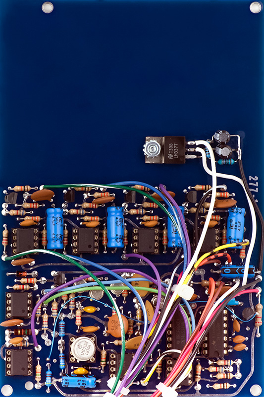
PCB1 contains all of the circuitry except the shift registers and clock drivers. I added the LM337 -10V regulator in the extra space and the small blue wire and missing components are part of my Sigma-Delta and level shift modification.
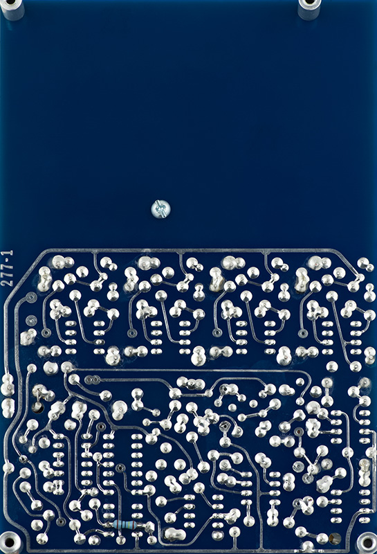
PCB2 contains the 48 shift registers and clock drivers. The -15V RC filter is the tantalum capacitor and a 220R resistor.
Initial Operation
I got the module to operate with a simple 1 bit digitization which results in the output signal always at full amplitude. Different delay outputs can be fed back to create echoes but careful adjustment of the mixer is required to prevent the 277 from self-oscillating at low frequencies. This video shows the initial operation with simply converting the input signal to a pulse waveform.
Sigma-Delta A/D and Shift Register Clocks
The Sigma-Delta A/D did not function as drawn and the component values shown do not provide a symmetrical bipolar signal from the 1 bit delay. Photos of 277 PCBs show different resistor values but they do not provide a functional bipolar signal either. This is a pretty simple Sigma-Delta converter and there certainly was room on the PCB to use an op-amp integrator with a proper summation amplifier, and a better 1 bit D/A.
Don implemented the integrator with a RC network to ground and added the feedback signal to the input signal at the negative input of the comparator. The subtleties of this circuit are to balance a proper data level for the shift register, not exceeding the drive capability of the 7400 gate, providing a symmetrical bipolar delayed signal with proper summation for the comparator, and integration over the range of clock frequency.
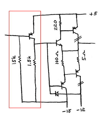
The first issue I noted is the current for the switching transistor Q16 exceeds the source capability of a 7400 gate. The schematic also shows this shorted to +5V. I suspect Don added a pullup resistor and a 3K resistor is within the sink capability of the 7400 and provides some additional source current.
I modified R41, R42, and R43 to provide a +/-4V signal from the output of IC7/Q16. I chose +/-4V since this is the output level of the input buffer with a +/-2V input signal.
One of the issues with this architecture is the integration capacitor is based on the switching frequency, but the switching frequency is variable. I selected a much lower integration capacitor to provide a reasonably useful level based over the frequency range. I changed R39 to provide a good summation with the input signal. The result is a reasonable Sigma-Delta pulse train as shown here.
The data high voltage is a bit above the maximum input voltage of a 1404A shift register but Don added a 3K3 resistor in series to limit current which is not shown on the schematic. There is also a pulldown resistor to -15V on PCB2 which would attenuate the data signal but I chose to leave it off.
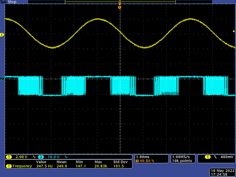
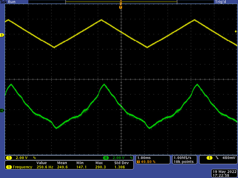
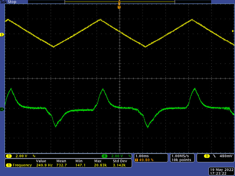
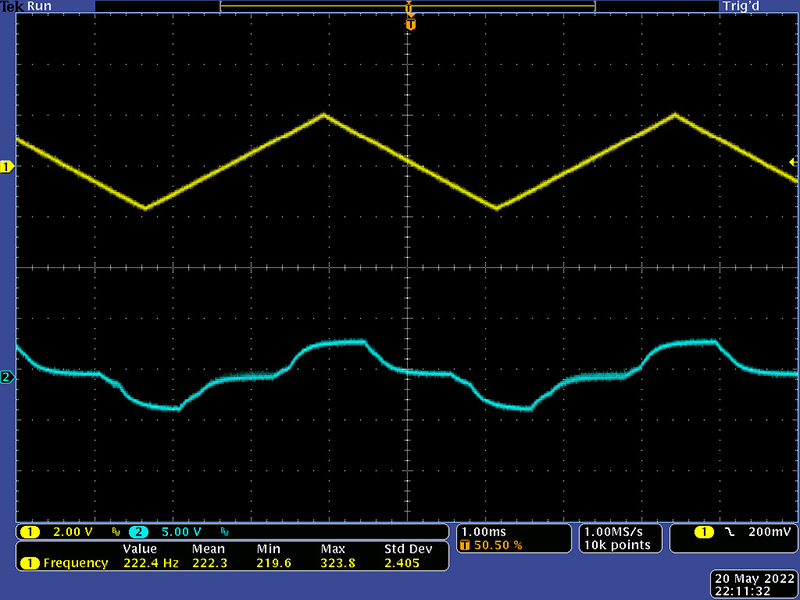
To begin investigation of the Sigma-Delta A/D, I bypassed the shift registers and fed the pulse train directly to the output filters to verify operation. There is a 4K7 pulldown resistor to -10V on the last shift register which attenuated the signal a bit. The filters show a reasonable output signal at the minimum delay time. These next scope photo pairs show the output signal on the panel jacks at minimum and maximum delays with no shift registers. The delay time simply affects the Sigma-Delta clock rate and integrator.
A sine input shows considerable distortion at the maximum delay. The input signal level can be adjusted to improve this a bit.

A triangle input shows similar degradation at the maximum delay.
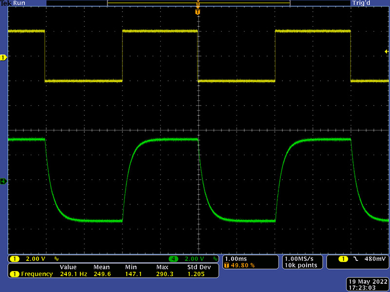
A square wave shows no difference between minimum and maximum delay since the pulse train is the same.

Moving on to the shift registers, the Ø
I don't know if this was a bad DSC0025 or a counterfeit so I wired up a DIP header with a discrete driver taken from the earlier June 27, 1972 277 schematics to fit into the DSC0025 socket.
The resulting Ø
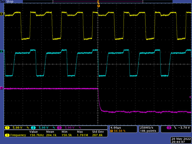
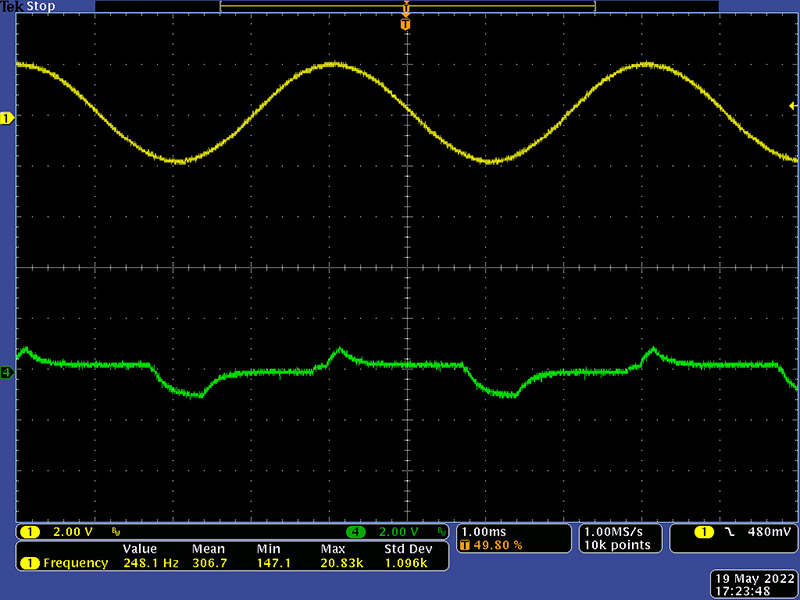
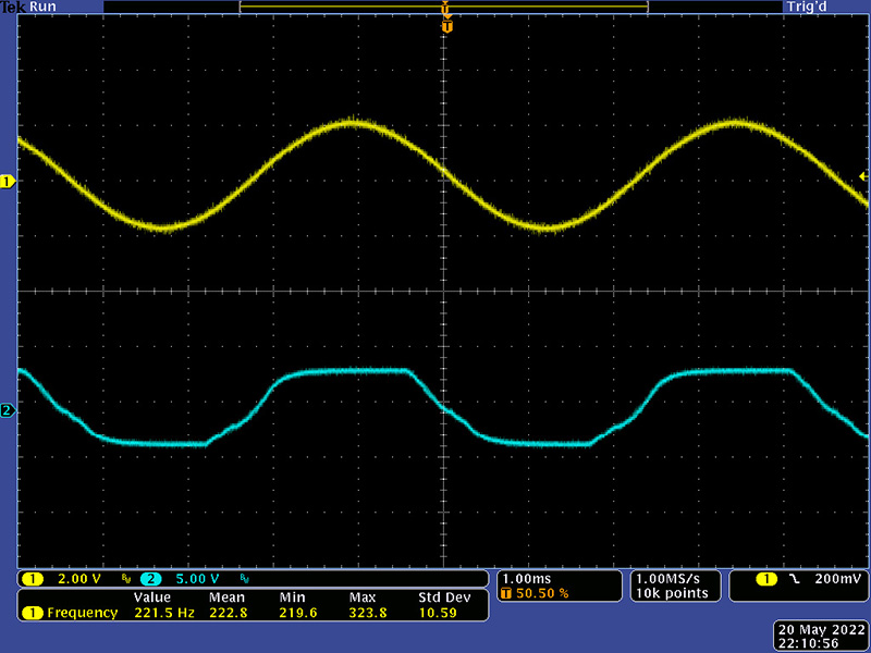
The result was a functional 277! The waveforms are degraded over those without shift registers. These scope photos are the outputs from the 4th T stage at minimum and maximum delays.
Sine wave.
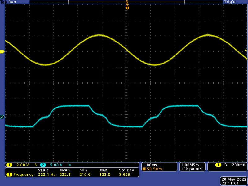
Triangle wave.
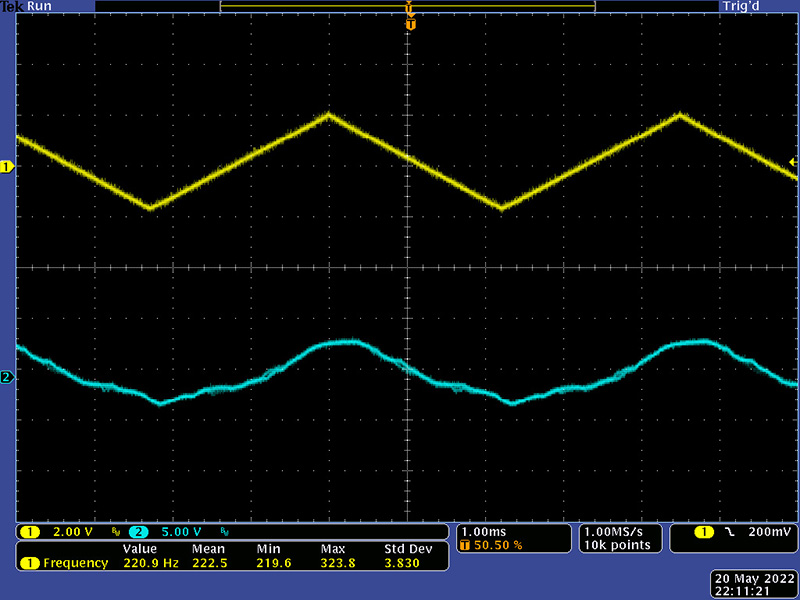
Square wave.
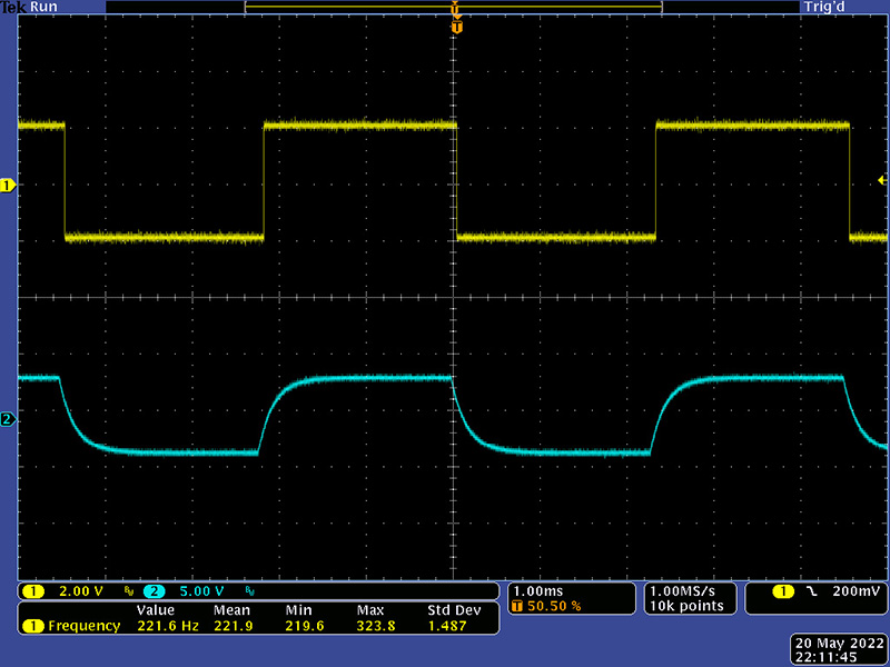
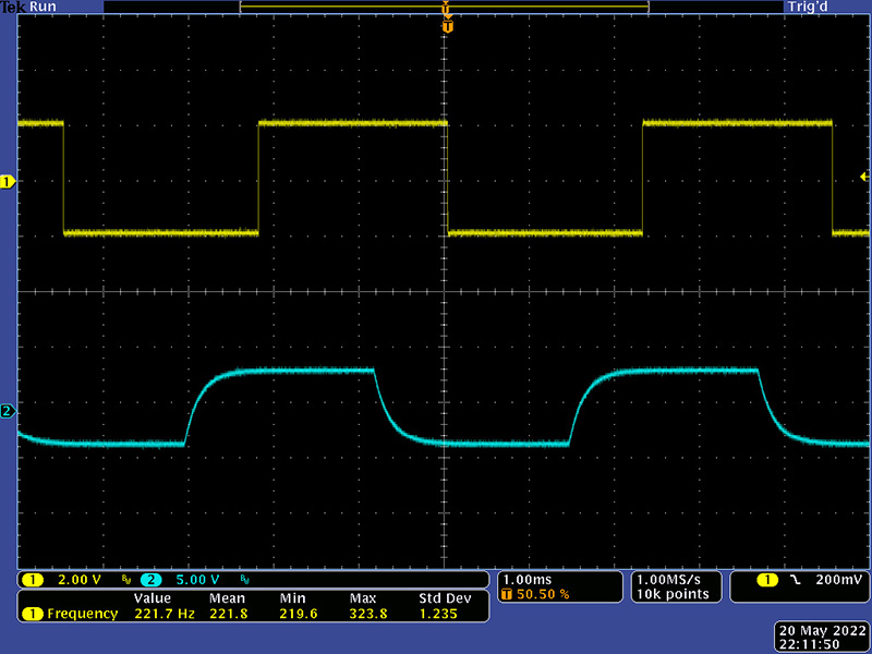
The square wave obviously has the least distortion. Although the sine and triangle waveforms are distorted they sound better than they look.
The overload LED is a comparator to the voltage on the input of the Sigma-Delta A/D. The integrator is fixed so n longer delays the voltage rises to a higher level. This makes the overload LED a bit finicky. I adjusted the threshold by changing R28 so it operated reasonably well on minimum delay. I set the overload LED threshold to where the feedback self-oscillations stopped. I suspect moving the comparator to the input mixer output might function better.
A quick measurement using a slow low duty cycle pulse indicates the minimum delay is 105 mS and the maximum delay is 366 mS, basically 2X what I calculated. The Sigma-Delta A/D runs on 2X clocks but the maximum delay is determined by the clock rate and number of bits. I don't have a good explanation of this yet.
Stability Issues
The VCO has become unstable above 230 KHz which corresponds to a CV of ~0V. With everything now functional there is a lot more noise throughout the system. The Sigma-Delta A/D runs on both clock edges and the 48 shift registers clocks now have steeper rise/fall times. At the maximum frequency, the triangle core is at the lowest amplitude and the waveform has ripples corresponding to the noise. There are wires running everywhere on this module and there is no power supply decoupling.
When the VCO becomes unstable the output has some white noise. The originals are reported to be noisy also, with white noise. The outputs become noisy if the input level is right at the comparator threshold and increasing the input signal reduces this noise. Using feedback increases the noise as there are now more signals at the comparator threshold.
I added 0.1 µF decoupling capacitors to every IC on PCB1 and three per row for the shift registers. The VCO is more stable now.
Power
The power requirements for the -15V is significant due to the
number of shift registers. The data sheet specifies that the current increases
with duty cycle of the Ø
| Supply | Current |
| +15V | 25 mA |
| -15V | 315 mA at minimum delay |
| -15V | 154 mA at maximum delay |
| +5V | 40 mA |
I could modify the shift registers back to -15V operation. The LM337 does provide some isolation for the -15V supply. Operating at -15V, the Vil specification for data is -10V maximum which is right at the output level of the Sigma-Delta A/D which would require some modifications. The shift register termination resistors specified in the data sheet for 14V operation (+5/-9) are 6K2 instead of 4K7. There is no mention of shift register maximum operating voltage, only +5V +/-5% and -9V +/-5%.
Operation
Here are two cell-phone videos of operation. This video is a
fixed frequency input signal with FM modulation to create vibrato. The oscilloscope
is displaying the shift register Ø
This video is a swept triangle signal with feedback of the T signal at maximum delay. The oscilloscope is displaying the input and T signal output.