|
264M Quad
Sample & Hold |
|
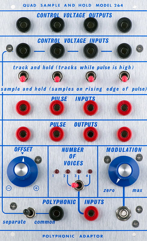
The 264 Quad Sample & Hold consists of four independent sample & hold circuits which can be configured to either sample on the rising edge of the pulse or track for the duration of the pulse. Each of the outputs can be modified by the Offset control and FM modulation.
The polyphonic support consists of two independent functions - a separate/common CV switch and 2 to 4 stage pulse generator. The switch simply disconnects the four CV input jacks and connects all four sample & hold circuits to the common CV input. The 2 to 4 stage pulse generator generates sequenced pulse outputs from a common pulse input. The Pulse Output jacks need to be connected to the Pulse Input jacks for the number of voices selected. With the switch in the Common position, the CV sampling is then sequenced through the number of stages selected.
For example, on the first pulse, the CV is sampled and held in the first channel. On the second pulse the CV is sampled and held in the second channel. When the maximum number of voices is reached, the sampling reverts back to the first channel. Thus a CV can be sampled and routed along with its associated pulse input to four VCOs and sustained over the number of voice pulse inputs. This differs from an analog shift register where the CV to a particular VCO is maintained only for the duration between common pulses.
When set to 2 or 3 voices the additional shift registers may be operated with their own pulse input but their CV input is common as controlled by the switch. Note also that the Common switch need not be used with the pulse generator. This allows sequencing of the sample & holds with separate CV inputs.
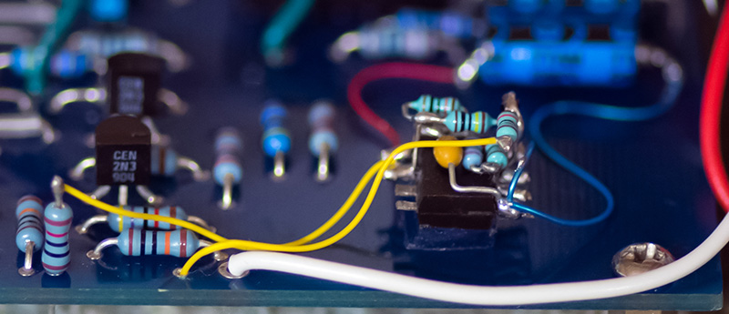
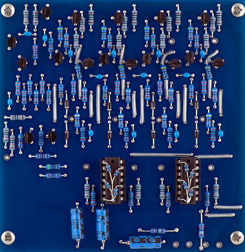
The panel wiring is complete prior to adding the PCBs. The in-line terminal strips are difficult to find so I fabricated both from 6 lug strips. The 9 lug is two strips pieced together and the 5 lug is shortened one terminal. I also used a terminal strip between two banana jacks for the ground connection to the resistors as it was better than trying to use the far left terminal strip. The left terminal strip is for routing power to the two PCBs.
I eliminated the +24V supply so the red wire connects +24V for IC4 to +15V and the zener is replaced with a 0R resistor to supply -15V. See modifications below for details.
PCB2 uses the MC846 DTL quad NAND gates which have internal resistor pull-ups. These are a somewhat rare and the leads are typically corroded so I use 74LS03 open collector with 1/8W 2K4 resistor pull-ups. All transistors are 2N3904 and 2N3906.
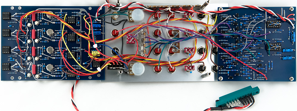
I wired the PCBs so they folded to opposite sides to be accessible for service. Construction of this module was quite tedious.
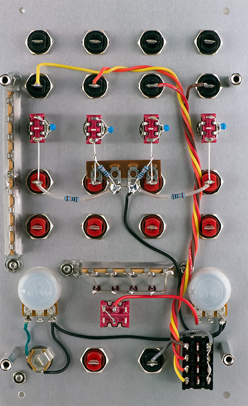
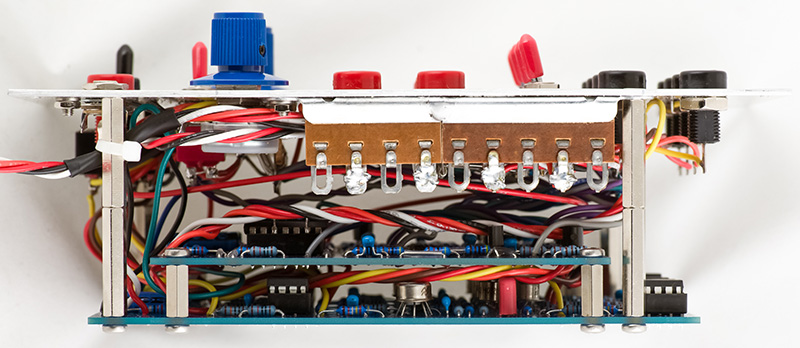
The boards fold together and make a very compact and dense module. The shorter standoffs are 12 mm to allow clearance for the LED terminal strip.
Operation
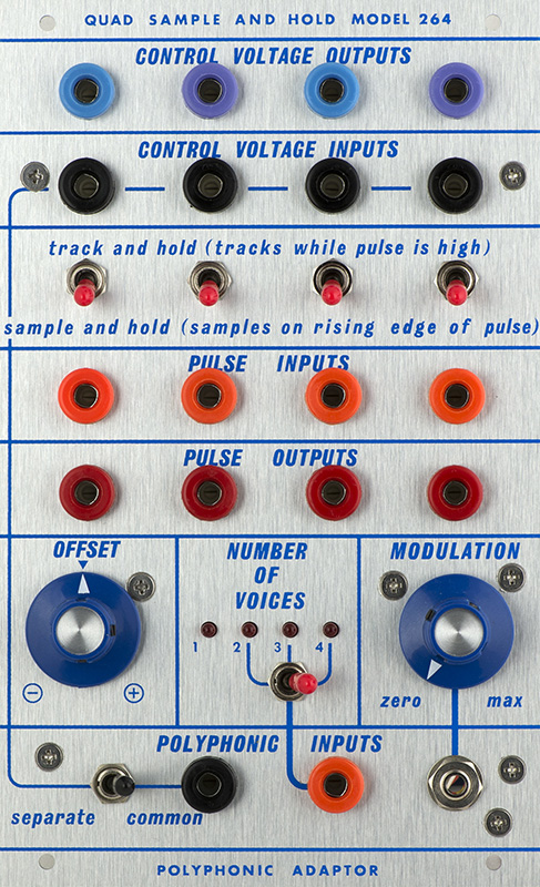
This image shows a single channel sample and hold with no offset.
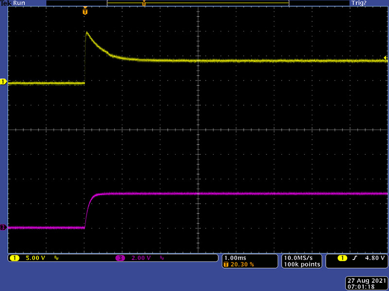
This image shows a single channel track and hold with no offset.
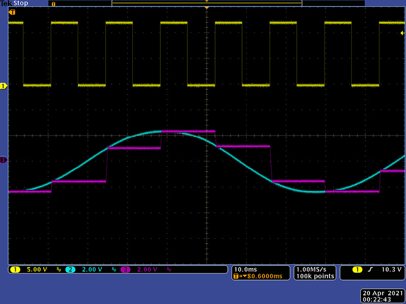
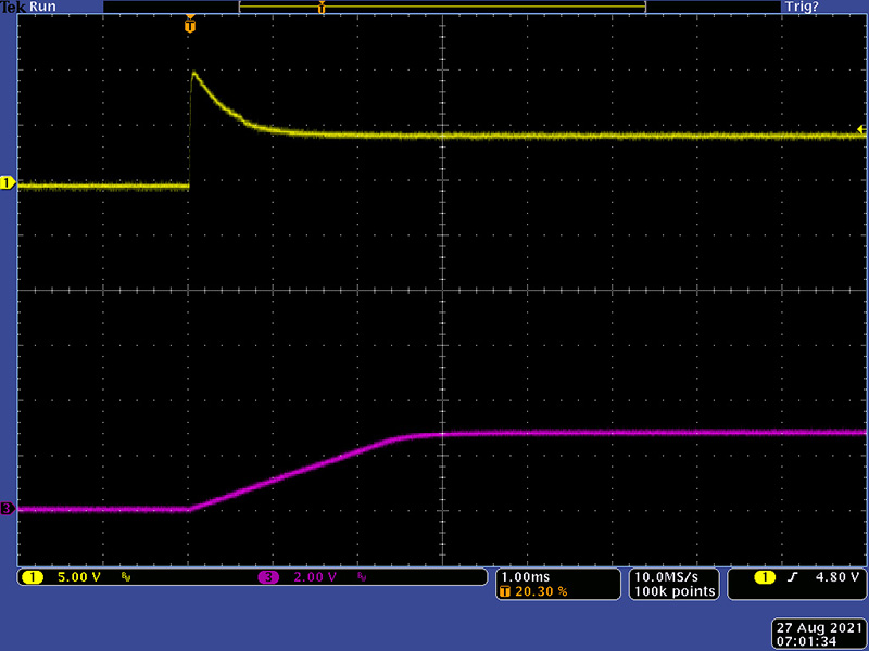
This image shows a two stage polyphonic sample and hold with no offset.
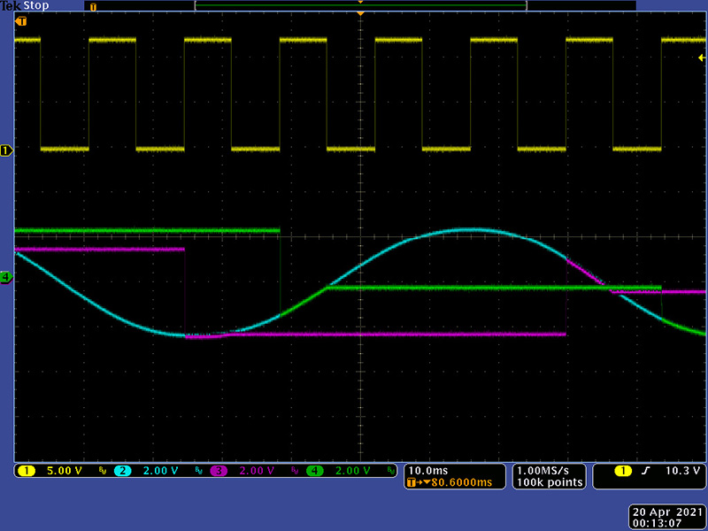
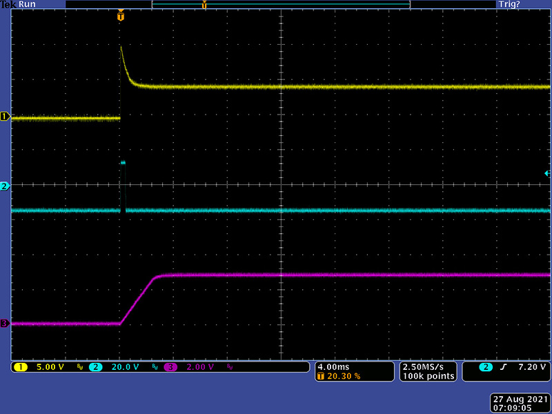
This image shows a two stage polyphonic track and hold with no offset.
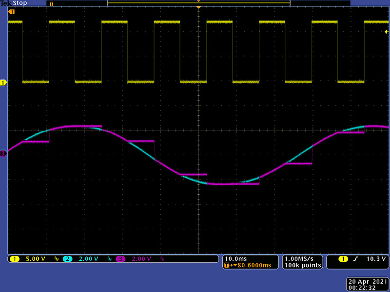
This image shows a two stage polyphonic track and hold with negative offset.
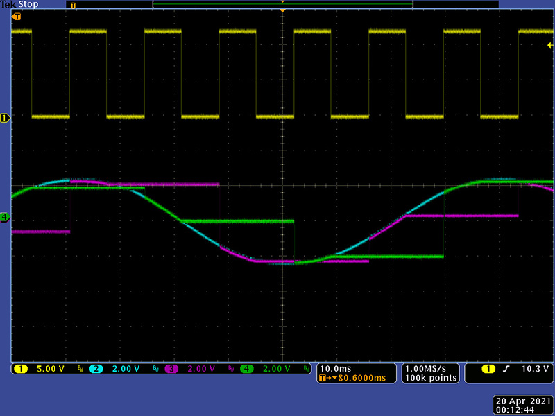
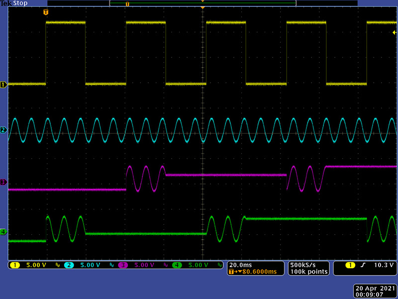
This image shows a higher input frequency two stage polyphonic track and hold with no offset.
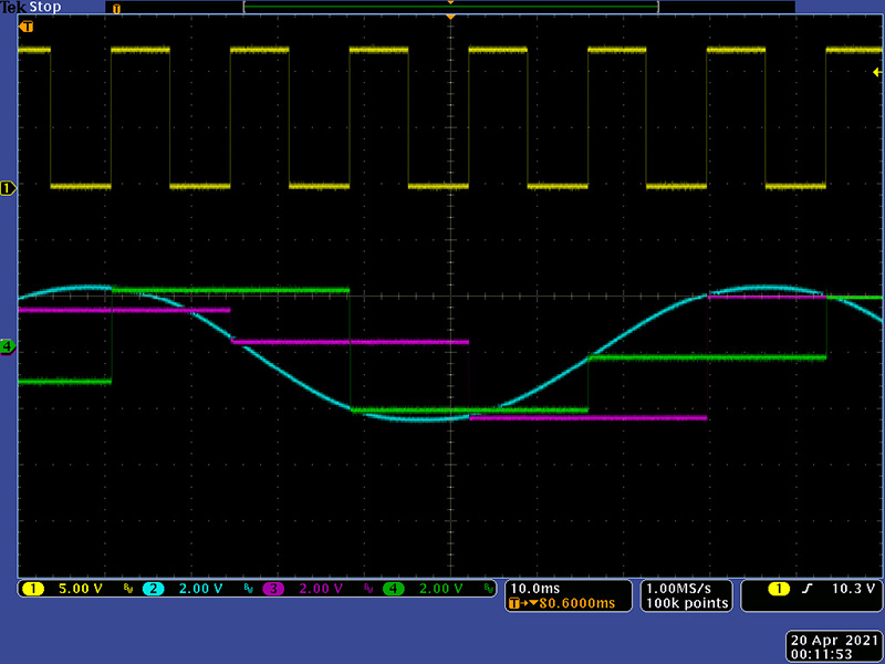
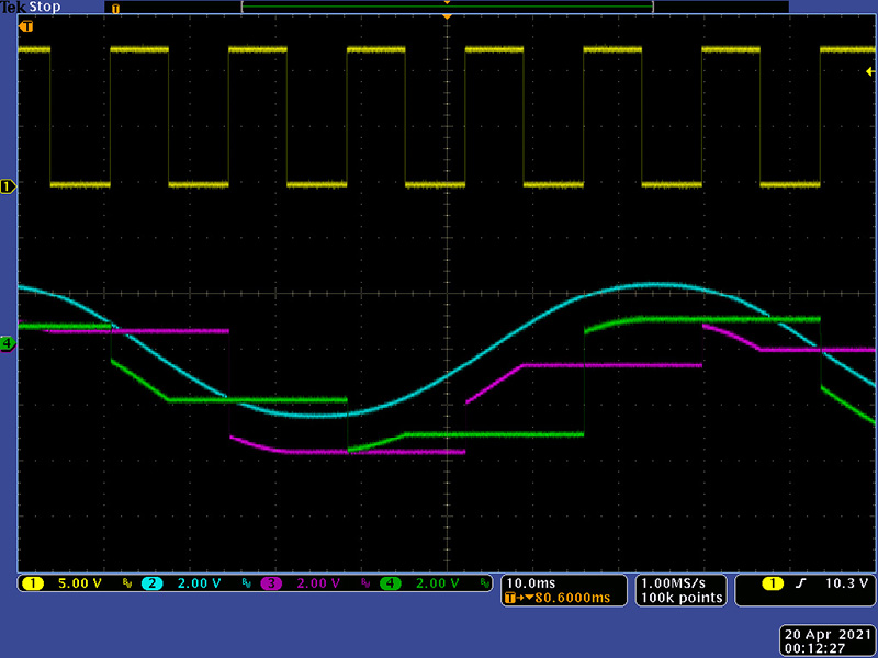
This image shows a four stage polyphonic track and hold with no offset. Only the first two channels are shown on a four channel scope. You can see the two pulse gap in the magenta and green traces where stages 3 and 4 are.
The module will not function as an analog shift register by simply patching a CV Output to the next CV Input. Like all sample and hold cells, they are really track and hold cells. "Sampling" occurs when the control pulse is sufficiently narrow to make the tracking time insignificant.
Analog shift registers work instead by using analog switches to route inputs and outputs to and from each cell. On each pulse the CV input is switched to the last cell in the sequence and the outputs are switched to provide the correct sequence. Only one cell is ever sampled at a time. A pulse counter controls the switch sequencing.
For example, on the first clock pulse the CV input is switched say to cell 1. Cell 1 is switched to output 1, cell 2 is switched to output 2, etc. providing the correct sequence. On the next clock pulse the CV input is switched to reuse the last cell which in this case would be cell 4, and cell 4 is switched to output 1. Cell 1 is switched to output 2, cell 2 is switched to output 3, etc. providing the correct sequence.
The control pulse on the 264 is 424 µS which provides adequate time for the sampling capacitor to reach the desired voltage.
Modifications
There are a number of issues with this design. In a 1.2V/Oct system, 5 mV is 5 cents which is the threshold of pitch variation. I was unable to reliably sample a fixed DC voltage and have a repeatable output. I had up to 17 mV of variation in sampled output.
The first issue was high frequency oscillations at the output of the LM301 CV buffer. I found that eliminating the 470K resistor and simply connecting the 22 pF compensation capacitor between pins 1 and 8 eliminated the high frequency oscillations. The LM301 specifies 30 pF but I simply used the existing 22 pF capacitors.
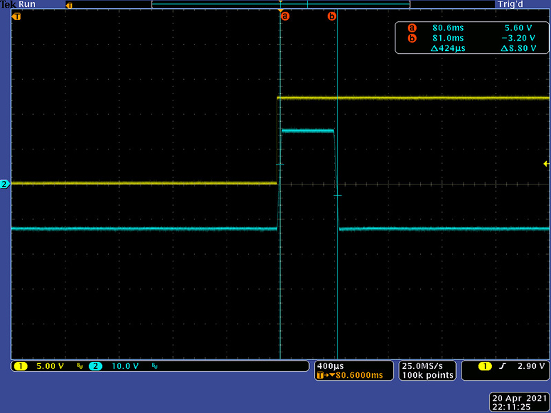
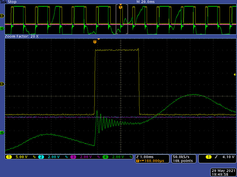
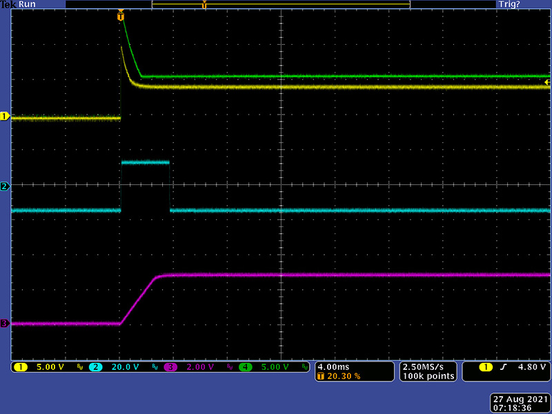
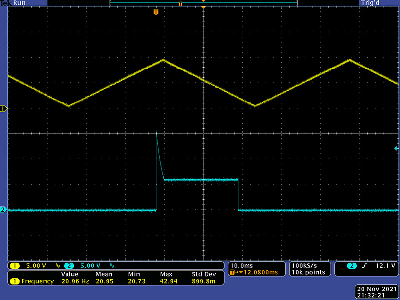
To compensate for losses in the JFET buffer, Don took the feedback for the LM301 after its output. However, this output is the sampled voltage. When the Pulse Input goes low the LM301 has no negative feedback and is unstable. Then when the Pulse Input is applied, it takes some time to stabilize which is about the same time as the sampling pulse. You can see the erratic behavior of the LM301 output (green) when the sampling pulse (yellow) is low in this scope image.
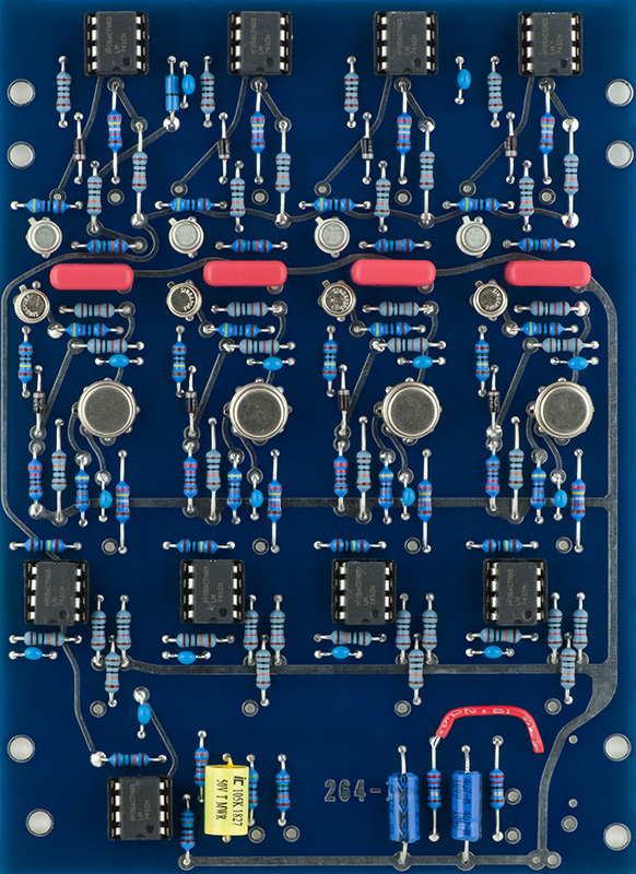
Sample & hold circuits have improved a lot in the 50+ years since this module was designed. Low bias op-amps and CMOS switches are now used eliminating the need for the JFET follower. I removed R15, R21, R22, and Q2. I connected IC3 pins 2 and 6 to for the negative feedback.
I changed IC4 to a CA3140 op-amp and changed the supplies from -5V/+24V to +/-15V. Pin 8 is a strobe input and needs to be lifted since it is connected to pin 7. I also lifted pin 3 and ran a wire over to the gate pad of Q2. This removes the sampled capacitor voltage from the PCB to minimize leakage to other traces. Normally there would be a guard ring around this trace.
These changes eliminate the erratic LM301 behavior and improved droop. My initial measurements showed a significant improvement in droop but later measurements show less but still an acceptable and improved amount of droop.
The CV Out range is +11.9V to -5.4V. The AD820A rail to rail op-amp should increase the upper voltage limit but 11.9V is very adequate at nearly 10 octaves.
The offset voltage of IC3 and IC4 can contribute to a perceivable pitch error on the output. I added a 3/8" trimmer on the back of the PCB to IC4 pins 1, 4, and 5 to be able to trim the output offset to less than 1 mV.
The CV input is attenuated by 20% and the output has gain of 1.25X. The resistors are 1% resulting in a gain error of up to +/-4% in the CV Out. At a 6.0 volts this can amount to 240 mV of error, or two semitones. I replaced R25 with a 22K6 resistor in series with a 1/4" trimmer on the back of the PCB to adjust the scale to exactly 1.0X.
The Offset control is an oddity. For some odd reason Don biased the + input of IC1 to 2.5V. This results in significant added voltage to the CV Outputs when the control is centered. This makes no sense to me. I chose to rewire the circuit so the Offset control runs on +/-15V so center is 0V. However, finding the center is near impossible so there is always some voltage offset applied. I replaced the Offset control with a 10K with a DPDT pull switch and wired it so the offset is inactive unless the knob is pulled out. This control has a range of +/-1.8V and will drive the CV negative.
The result is a very precise and usable module. Subsequently I did some more modifications document in the Epilog which are also included on PCB1.
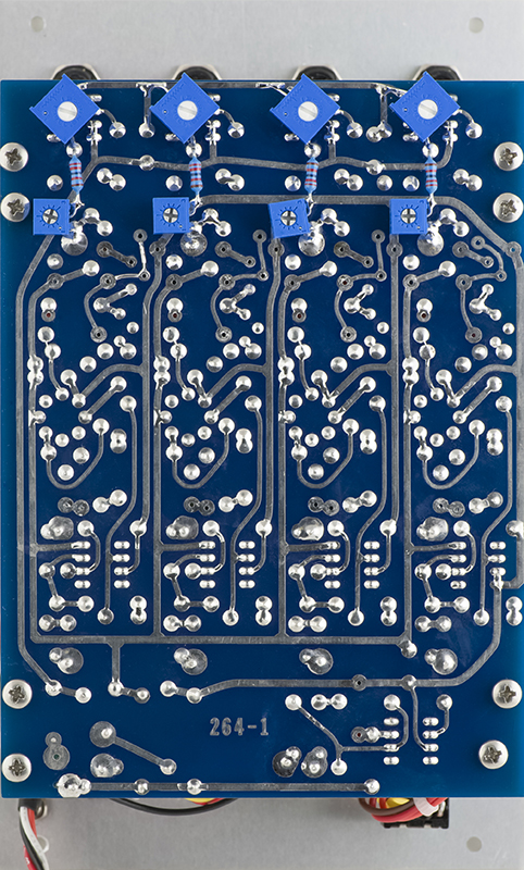
The Alpha potentiometer fits perfectly in the space using 12 mm standoffs for PCB2.
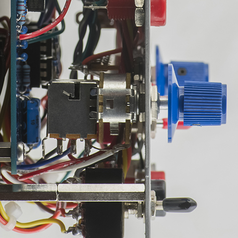
The trimmers fit nicely on the rear. The 3/8" trimmers sit slightly off the PCB connecting to IC4 pins 1 and 5 with the wiper to the -15V trace. The 1/4" trimmers fit flush to the PCB with room for the 22K6 resistors.
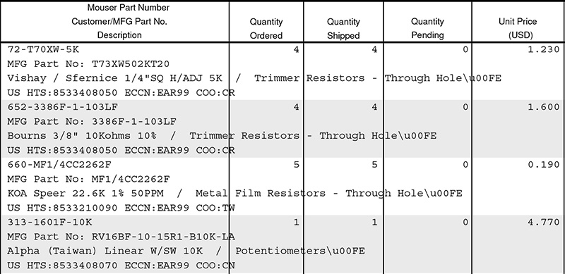
I already had the CA3140 parts (Mouser 968-CA3140AEZ) so these are the Mouser part numbers for the trimmers and potentiometer.
Epilog
This module was built with the modern 200 series color scheme which looks quite nice.
This 264 exhibited an issue in Poly mode where channels 2 and 4 would track and hold properly but in sample and hold the outputs were low. I used J203 JFETs in this build and I suspect they required a wider sample pulse. I increased C2 (x4) from 1 nF to 4n7 to address the issue.
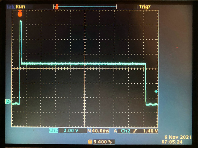
Later I found that driving it with my 218r exhibited some more tracking problems. This is the Pulse and Output from my 218r and is how I tested the 256 module.
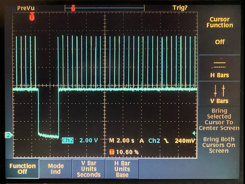
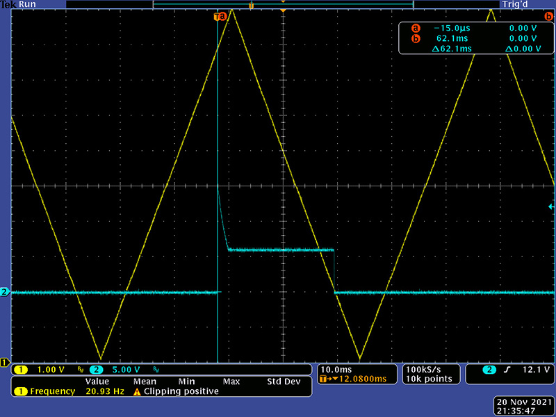
I found that the Slope Output with the portamento control set to minimum has considerable more slew.
The result which this image shows is sampling the CV (cyan pulse) while it is slewing.
I changed the differentiation capacitor C2 (x4) to 33 nF to increase the sample pulse to 4 mS. The output tracks during this pulse time but it is so short as to be negligible. I also found that the polyphonic pulse outputs had quite a narrow trigger pulse. I increased the pulse generation capacitors C4 and C7 (x3) on PCB2 to increase the trigger width (green) to be comparable with the 218 pulse output (yellow). This corrected sampling issues when using the 218r Slope Output.
I also wanted to minimize the current drawn by the polyphonic circuitry. LEDs are much more efficient now than in 1970 so I decreased the current by changing R27 (x4) to 1K. This drops the LED current about 30 mA. The resulting stability on the second polyphonic pulse for a channel with a significant initial change in CV input is now inaudible. However, if I use the 218r slope output I occasionally get a change on the second channel pulse. I don't want to increase the sample pulse width any wider and it doesn't make a lot of sense to sample a slewed CV for accuracy. I'll consider these as final modifications for use with my 218r.
I had one other strange occurrence during testing. IC2 on channel 1 failed in a mode where it functioned but had significant output slew. A replacement 741 also failed in the same matter. For some reason pins 7 and 8 are tied together only on channel 1. Pin 8 on a 741 is supposed to be no connect but lifting it seemed to eliminate failures. This module ran for weeks with those pins tied together and it shouldn't matter anyways - very strange. Note that pins 7 and 8 are also tied together on IC4 which was a problem with the CA3140 as that is the strobe input.
264 Operation With A BEMI 218e
My customer reports using a 218e will not trigger the polyphonic input. He can run the 218e pulse through other modules and those pulse outputs will operate the polyphonic input. I believe this is related to the rise time of the polyphonic pulse input which uses discrete transistor circuitry.
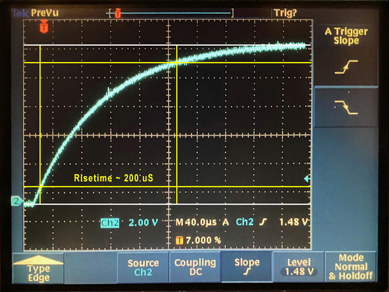
Steven Barsky sent me these images of his BEMI 218e outputs. The trigger portion is a ~4.5 mS 11V pulse with a 5.5V gate.
The pulses from the arpeggiator function as one would expect with a constant gate for the duration.
The trigger rise time is ~200 µS which is too slow to trigger the polyphonic pulse divider.
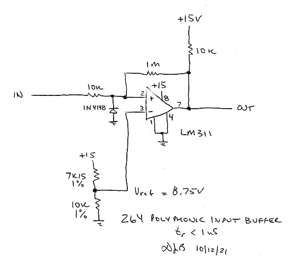
Adding a LM311 comparator to process the polyphonic pulse input and with a threshold of 8.25V will work with both the 7.5/15V and 5/10V pulse levels. This has to be added for just the polyphonic pulse divider as other circuitry holds the output gate for the duration of the input gate.
Looking at the CV with respect to the pulse shows a second issue as the CV is not stable during the trigger. This works when using the 218e as a CV source as the duration is short. one can almost think of this as a 4 mS delay followed by 4 mS of portamento. When using the polyphonic support the CV needs to be stable for sampling to be routed to the appropriate VCO. However, my customer reports that using the individual pulse inputs the CV samples correctly. There were numerous modifications to the 218e so perhaps this issue was addressed.
One option to address this would be to increase the sample pulse width to 10 mS. Another option would be to add two additional delays using a CD4538, one to delay 10 mS until the CV is stable and another to generate a 4 mS trigger pulse for the polyphonic pulse divider. A third option would be to add an 8 bit microprocessor to the 218e to sample the pulse output and delay it 10 mS which is probably the best solution.
This is the LM311 circuit that I added to set the polyphonic pulse input trigger to 8.75V. I lifted R7 where it connects to R1 and added this circuit between with the In connecting to the PCB pad and the Out connecting to the lifted R7.
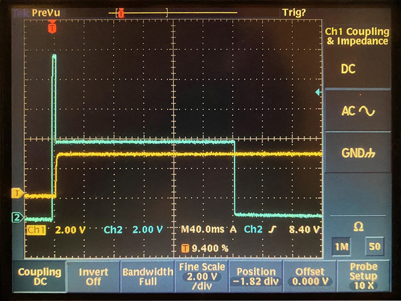
It performs as expected. This is the polyphonic pulse input driven with a 10V square wave.
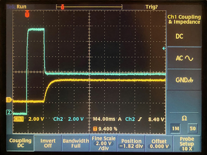
Changing to a triangle verifies correct operation with a slow rise time input.
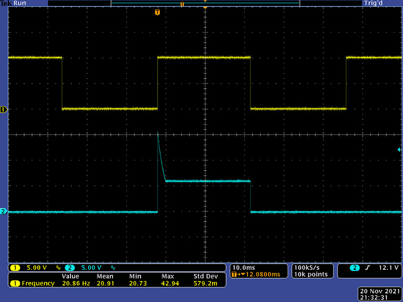
This image verifies the trigger sensitivity at 8.75V and the gate release at about 2V.
Lowering the amplitude to about 8.6V verifies the trigger level is below the threshold and the gate portion remains off.
Here is a photo of the modification using 1/8W resistors and mounting the IC on the top in the empty area of PCB2.