|
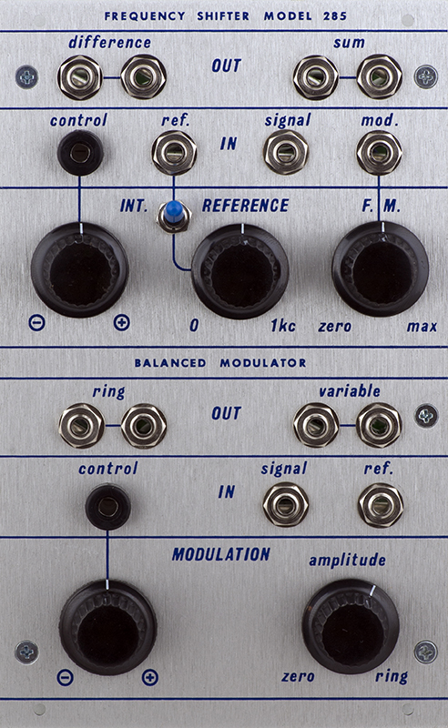
285 Frequency Shifter FV-1 |
|
I built this version for myself as I wanted to see how it performed. This version is designed around two of the Spin Semiconductor FV-1 reverb IC which can be custom programmed with an external eeprom.
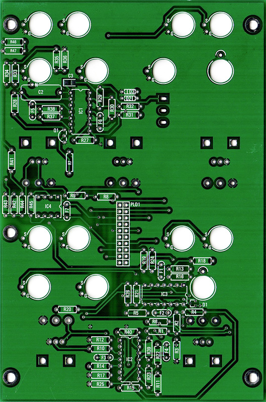
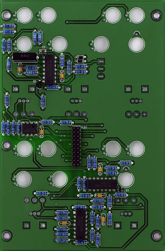
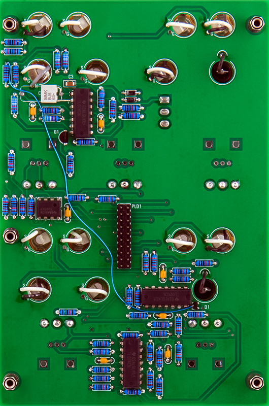
The FV-1 version consists of a two board set with a few surface mount components. PCB 1 has the front mounted potentiometers and a small number of active and passive components.
I made a reference diagram from the PCB image.
285 FV-1 PCB1 reference diagram
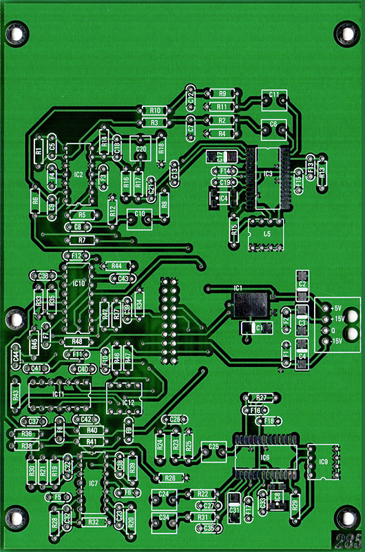
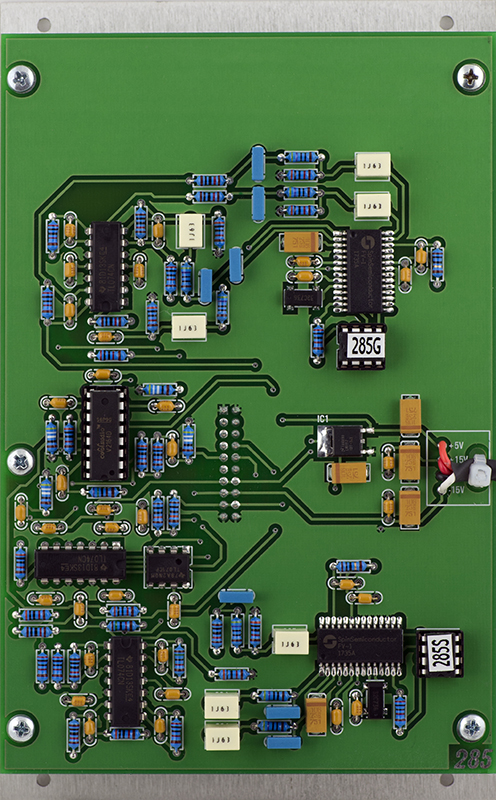
PCB2 contains the surface mount Spin FV-1 ICs and supporting circuitry. There is no calibration required for this module.
I made a reference diagram from the PCB image.
285 FV-1 PCB2 reference diagram
The build is relatively simple. There are a few SMT parts to solder. PCB1 does have a 2.7nF capacitor that I chose a film for that is nearly 12mm in height so close to the inter-board spacing. As typical with my builds, I insert the male pins into the female header on the back of PCB2 and use the standoffs to space the boards before soldering the header. This ensures the connectors are fully mated.
Mouser BOM Includes stock modifications and updated part numbers
I only used sockets for the eeproms and the V2164D. The eeproms have labels because I burned them.
Operation
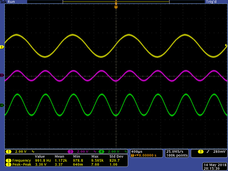
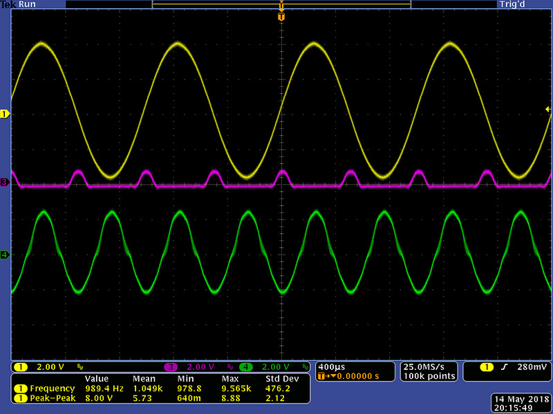
I didn't expect the performance of this to match the original all-analog frequency shifter. My first performance verification was to look at a frequency doubler by using the same sine wave for both signal and reference. I found that the signal level made a difference as to the resulting waveform. With a signal input level of 3.36V pk-pk both the Difference and Sum outputs show a frequency doubling with the Sum having a larger amplitude.
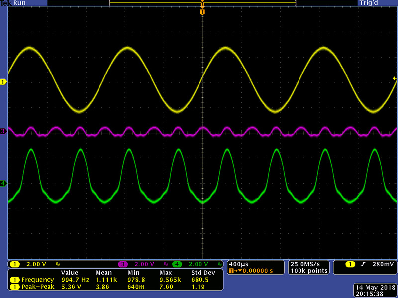
With a signal input level of 5.36V pk-pk the Difference output is beginning to flatten and the Sum output show a distorted frequency doubling.
With a signal input level of 8.0V pk-pk the Difference output has some small bumps and the Sum output show a less distorted frequency doubling.
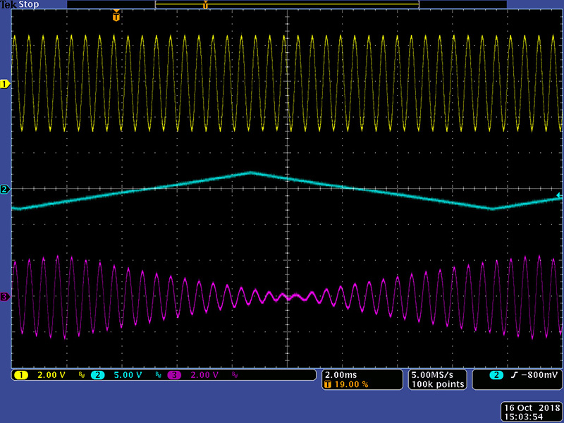
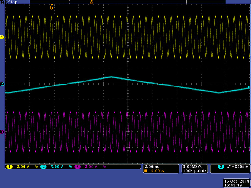
This scope image shows my best attempt at a frequency doubling using the internal oscillator.
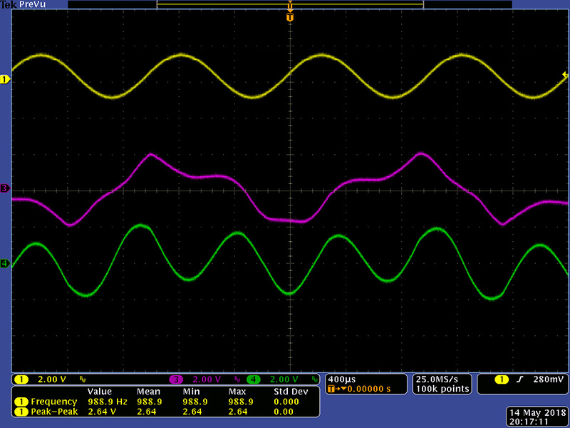
This scope image shows the variable output set to 0 and the ring output with 2.64V signal levels at a 2:1 frequency difference.
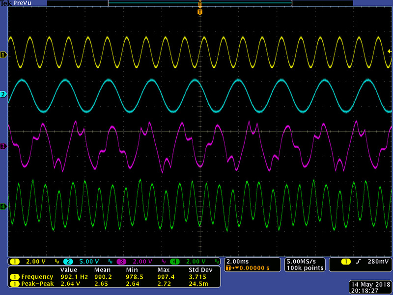
This scope image shows the variable output set to ring and the ring output with a 3.92V and 3.60 signal level at a 2:1 frequency difference.
While not as good as the original all-analog frequency shifter, the performance is reasonable and the sound qualities are quite nice.
Update
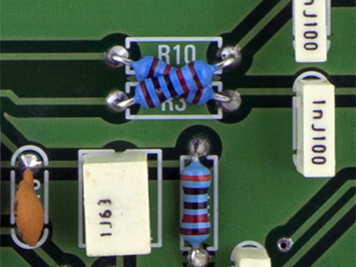
While repairing another 285 FV-1 I noticed a few discrepancies that I didn't notice before. I didn't pay much attention to the Sum and Difference outputs but they are backwards! It is an easy fix. Crisscross R3 and R10 on PCB2 to swap the outputs.
These scope photos show the corrected outputs. My input frequencies are 2021 Hz and 1547 Hz for a Sum of 3568 Hz and a Difference of 474 Hz. Measuring the green Difference output is a frequency of 474 Hz.
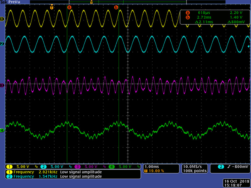
Measuring the magenta Sum output yields a frequency of 1/280 uS or 3568 Hz.
I also noted oddities with the FM control. With no jack inserted, the control is inoperative like one would expect. The circuit is actually normalled so the output of the FM circuit is 0V. When you break the normalled connection, the output jumps to 3V (for 3.3V logic) and the FM control attenuates this voltage so it acts as a secondary Reference control even with no voltage applied. When you apply a voltage to the jack, that voltage is subtracted from the 3V.
To prevent over-voltage to the Spin chip a BAT54S is used as a clamping diode to the supplies. However, this clamp is applied directly to the output of IC2 pin 14. The series limiting resistor is after the diode, not before. TL072 op-amps have short circuit protection but this diode should have been on the other side of R34. You can cut the run between the via and the left pad of D1. Run a wire from the left pad of D1 up to the junction of R33 and R34.
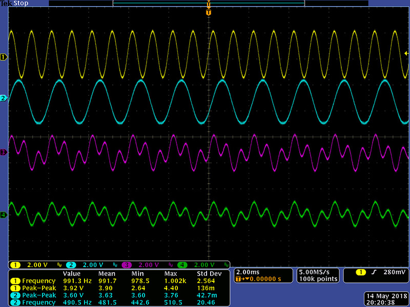
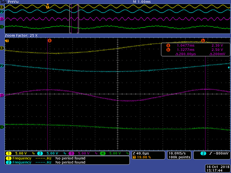
Here are some more scope images of the Ring Modulator. The yellow trace is the signal and at the Zero setting is output.
At the full Ring setting you get a four quadrant multiplier. Note the nulls are shifted from the Reference signal.

At the mid setting you get a 2 quadrant multiplier with less shift.