 |
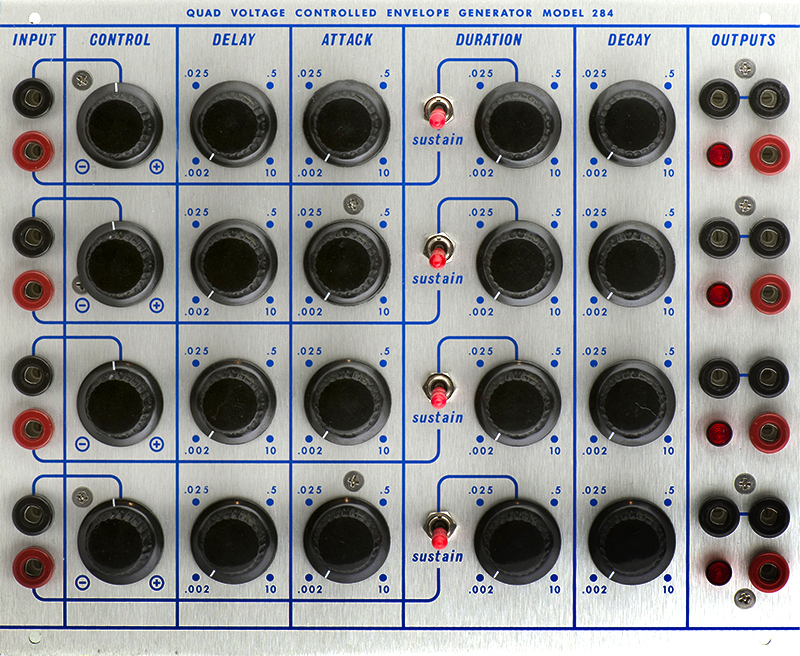
284 Quad VC Envelope Generator Module |
|
I built this 284 for myself.
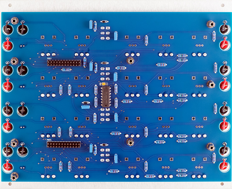
Here is the rear of PCB1. Since this design has low currents, I chose to not use any sockets so I could more thoroughly clean under the ICs.
PCB2 has a jumper for internal/external +24V and 8 trimmers.
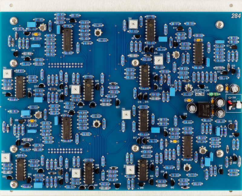
| Trimmers | Function |
| TR1 | Channel 1 Delay/Duration |
| TR2 | Channel 1 Attack/Decay |
| TR3 | Channel 2 Delay/Duration |
| TR4 | Channel 2 Attack/Decay |
| TR5 | Channel 3 Delay/Duration |
| TR6 | Channel 3 Attack/Decay |
| TR7 | Channel 4 Delay/Duration |
| TR8 | Channel 4 Attack/Decay |
Calibration
I set delay, sustain, and decay to 0 and attack to 10S. I could then trigger a channel and easily measure the length of the attack phase and calibrate it at 10 seconds. Then I set attack, sustain to 0, delay to 10S and decay to something short. I could then trigger a channel and measure the delay and calibrate it to 10 seconds.
With all four channels cycling and set to internal 24V, +15V was 160 mA and -15V was 75 mA.
Operation
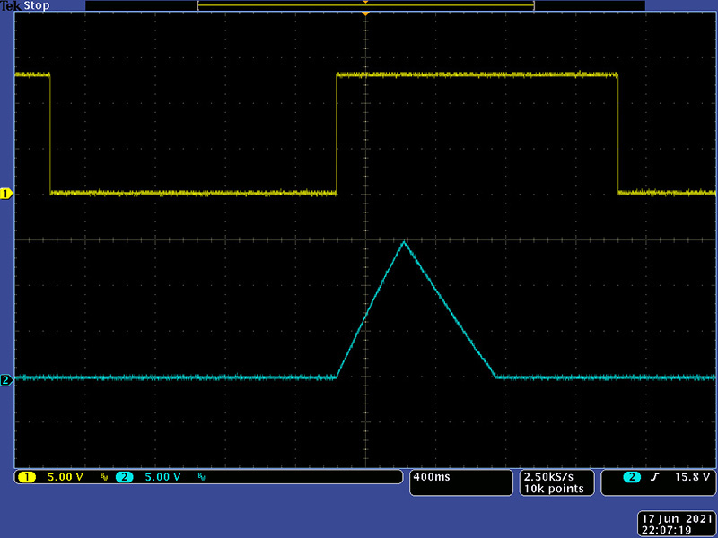
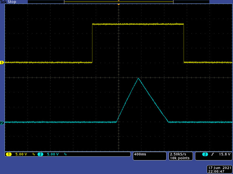
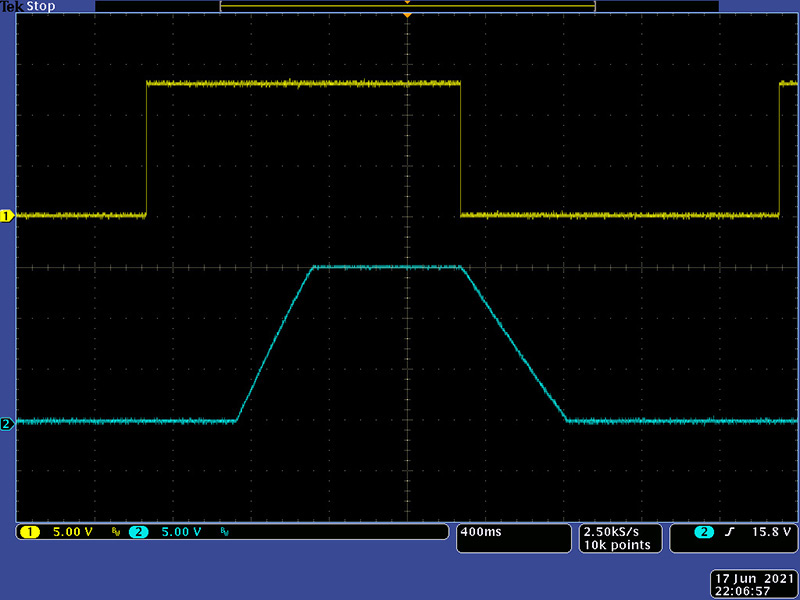
Here are some scope images of various waveforms. This scope image shows Attack-Decay with no Delay, Duration, or Sustain
This scope image adds Duration to show Attack-Duration-Decay with no Delay or Sustain
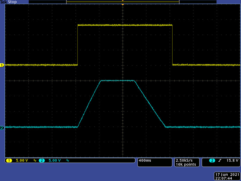
This scope image adds Sustain to show Attack-Sustain-Decay with no Delay
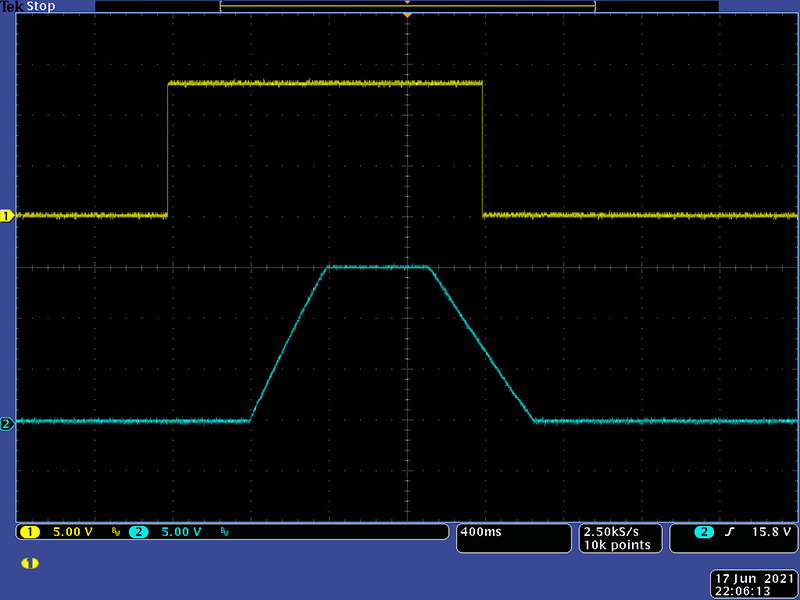
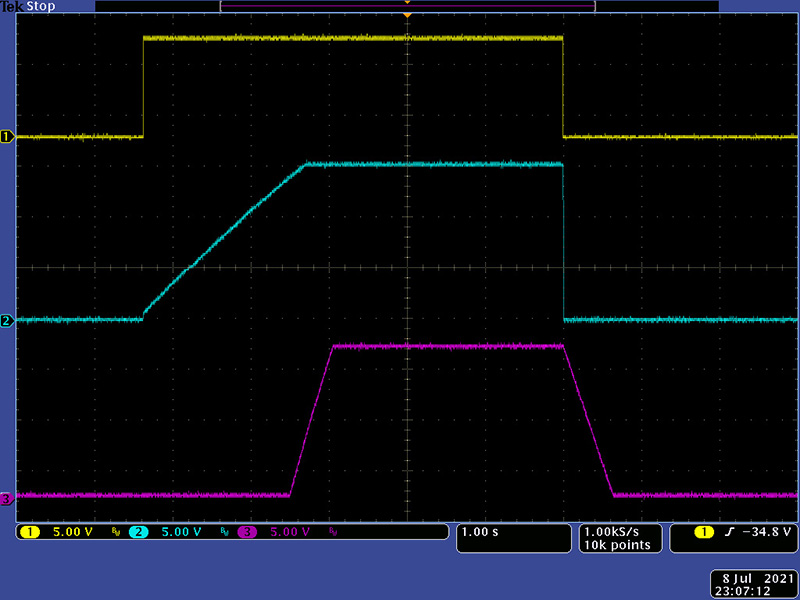
This scope image shows Delay-Attack-Decay with no Duration or Sustain.
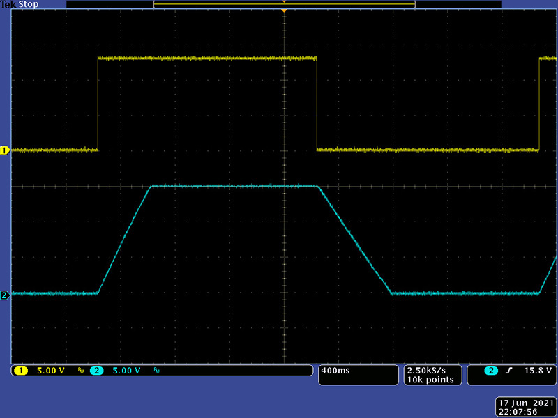
This scope image adds Duration to show Delay-Attack-Duration-Decay with no Sustain.
This scope image adds Sustain to show Delay-Attack-Sustain-Decay.
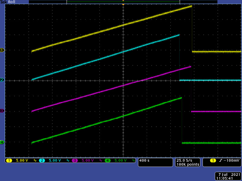
I spent extra care in building this 284. With the CV modification of the maximum times, I knew there would be very low currents and any leakage on the PCB would cause issues. I used cut tape transistors for matching, organic solder with frequent cleaning, and no sockets so I could clean around the legs of the ICs (which you can't do with sockets). The results are a very impressive maximum attack duration of over 45 minutes! I set delay, duration, and decay to minimum, attack to maximum, and used a +10V CV. I connected all four channels together with a single trigger and monitored the results. To me this is impressive for an analog delay and I don't know why anyone would want such a long envelope. Assuming the other three segments have the same duration, this would result in a 3 hour envelope!
Design
The 284 is an interesting design. It is comprised of two AR envelope generators operated in a loop fashion. The first envelope generator is for the delay and duration and the second envelope generator is for the CV output.
At the end of attack of the first envelope generator it triggers the second envelope generator and remains in a hold. At the end of attack of the second envelope generator it releases the hold of the first envelope generator (to start the decay) and remains in a hold. At the end of decay of the first envelope generator it releases the hold of the second envelope generator (to start the decay).
Since the second envelope generator has not started the attack, the attack of the first envelope generator creates the delay. Since the second envelope generator holds at the end of the attack, the decay of the first envelope generator creates the duration.
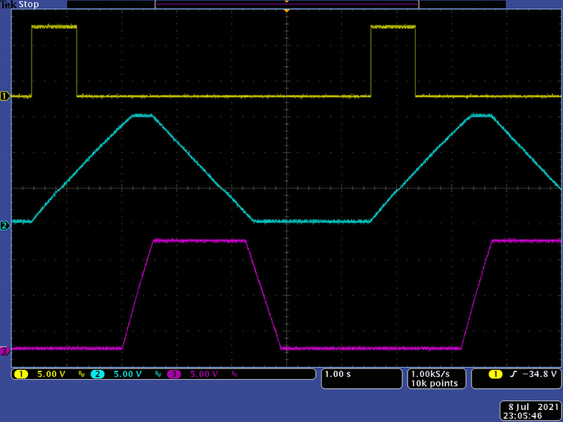
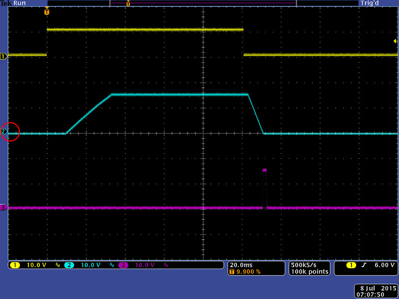
This scope image shows the two envelope generators. Cyan is the output of the first envelope generator at R35 (+ input of the op-amp). Magenta is the second envelope generator at R56 (+ input of the op-amp).
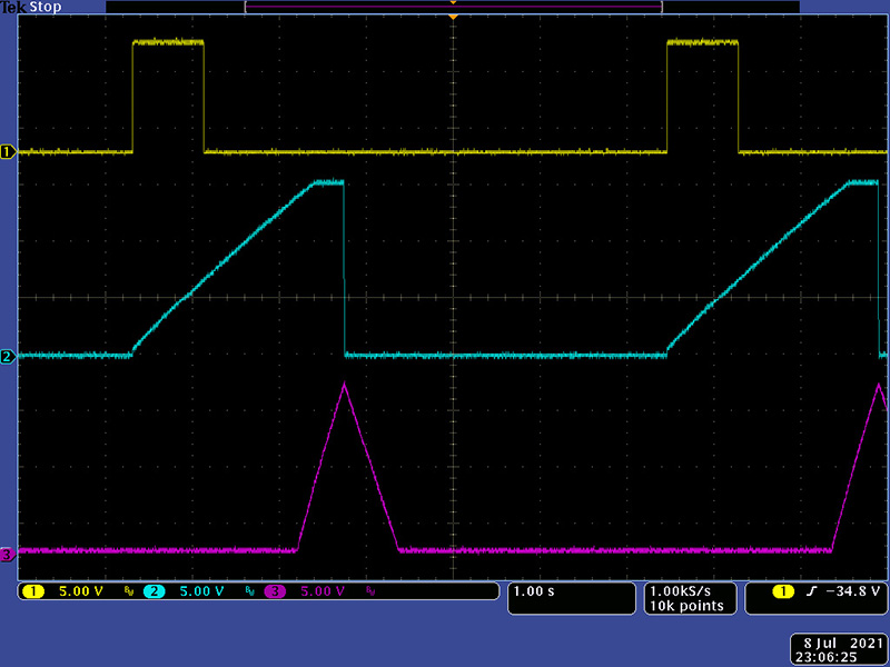
The sustain switch sets the decay of the first envelope generator to 0. This scope image shows sustain on but with a narrow trigger so the envelope consists of Delay-Attack-Decay
This scope image shows sustain on with a wide trigger so the envelope consists of Delay-Attack-Sustain-Decay
The CV input simply biases the dual pairs so more or less current is steered to the integrators.
Design Idiosyncrasies
I'm not sure where Don described the features of his modules. A customer contacted me about the CV outputs being negative when they are not generating a cycle. I hadn't noticed this before but this waveform clearly shows it. Although I lined the trace up with the graticule you can see that it is below the ground reference.
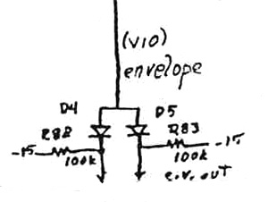
The 284 remains in the decay stage until a pulse moves it to the delay stage. In looking at the output structure, I noticed diodes in series with the CV outputs.
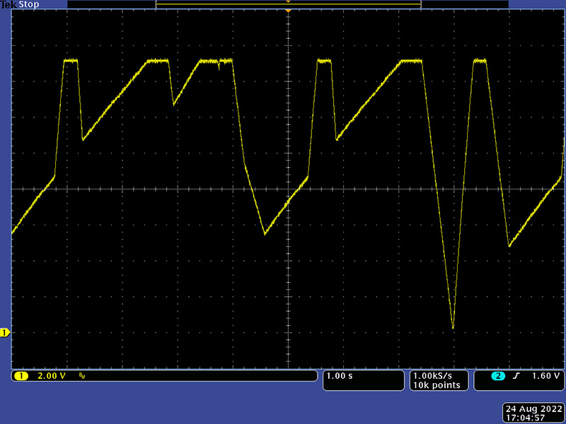
This means the outputs can be paralleled! This scope image shows the four outputs paralleled with a common trigger. Channel 1 is an attack/decay. The other three channels are shorter attack-duration-decay. They are positioned with a delay, the first two within the cycle of channel 1 and the third beyond the cycle so it is triggered every other cycle. The slight glitch is the beginning of a decay followed quickly by an attack. The clone CV outputs are wired in parallel with only one diode which limits the functionality. Wired the original way, one could parallel one output to create a complex waveform but use the other output as normal for just that channel.
Alternative 1:
Now back to the negative voltages. The CV output voltage varies between -0.8V and -0.1V depending on the setting of the Decay control. Rather than redesign the output stage, I decided to see if I could use this feature to "add-in" 0V to each output. I simply used a diode and resistor to create a 0.6V reference and the a diode to each channel to add-in 0V. I chose the resistor value to provide the correct voltage to compensate. With this arrangement the CV output voltage varied between -22 mV and +22 mV depending on the Decay control, a significant improvement from the -0.8 V.
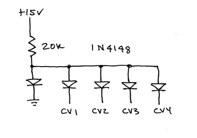
The downside of this simple modification is that when cycling, the current draw varies which changes the reference diode drop from 0.550 V to 0.600V. This 50 mV change is then added to the CV outputs.
With one stage cycling, the other three outputs vary from +37 mV to +42 mV depending on the Decay control setting.
With two stages cycling, the other two outputs vary from +66 mV to +70 mV depending on the Decay control setting.
With three stages cycling, the remaining output varies from +83 mV to +85 mV depending on the Decay control setting.
I decided this was good enough. Creating a regulated reference supply and matching it with the four diodes would be a more elegant solution. The output structure could also be redesigned but that is a more extensive modification.
Alternative 2:
I decided later I really wanted the independent outputs so I could use a normal CV output and parallel the other for complex envelopes. The diode and pulldown resistor are on PCB2. Replace D5, D10, D15, and D20 with a wire link. Remove R75, R151, R227, and R303.
On PCB1 replace the wires to the CV banana jacks with a 1N457 with cathode towards the jack. Wire a 100K to each banana jack and twist the other leads together for each pair of outputs. Wire these twisted junctions together. Per the schematic they should connect to -15V. I have no idea why Don did this and could see no benefit so I wired mine to ground which eliminates the negative output voltage. An individual sent me photos of his modifications using Alternative 2.