|
257 Control
Voltage |
|
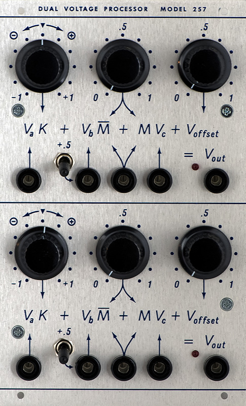
I built a 257 Control Voltage Processor module for someone else. They sent me a complete kit of parts and I assembled and tested the module. Many of the components are sourced through Mouser but specialized parts, panel, and knobs have specific sourcing requirements. Here is a photo of an original module.
There is only a single PCB in the module.
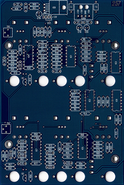
I made reference designators from the PCB images. The components cover the silk screen legends once populated which makes it hard to debug if anything is wrong.
PCB Front Reference Designators
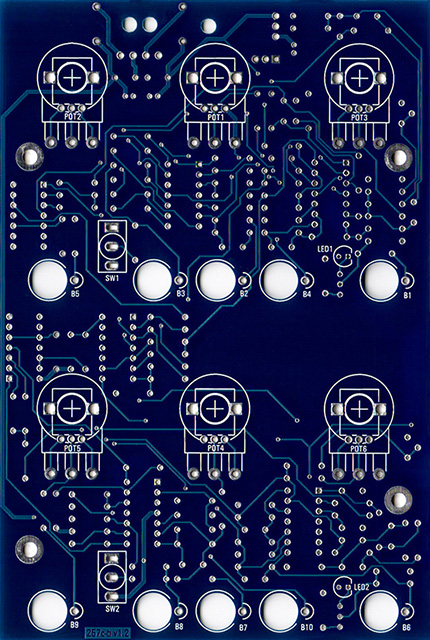
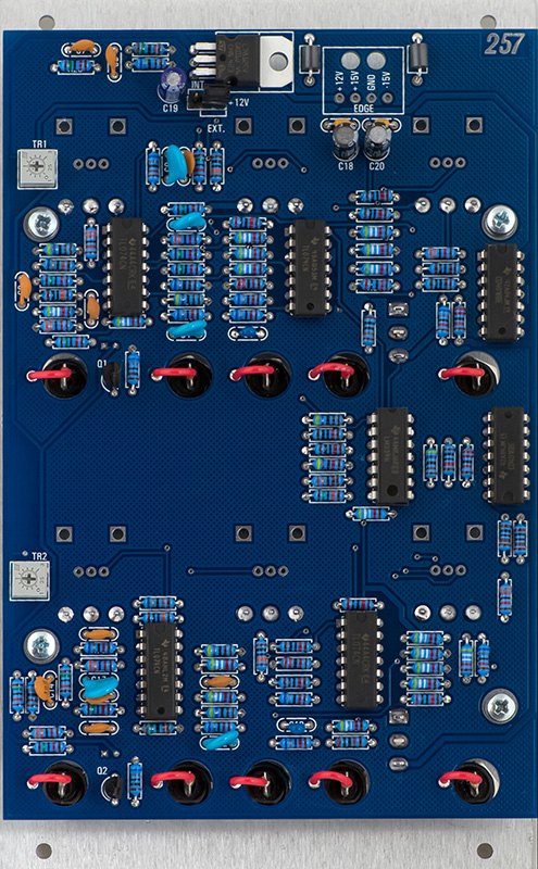
PCB Rear Reference Designators
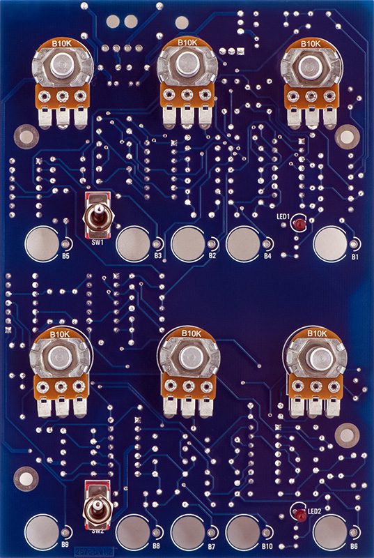
I've mounted the potentiometers and switches by soldering a single lug. After assembly I reflow the pin so the part will relax into the proper location. The LEDs are unsoldered and I push them flush to the panel before soldering.
Everything is finished except for the power cable.
Calibration
There are just two trimmers for offset on this module. Set the M (center) knob to the center and turn the Voffset fully counter clockwise. Measure the Vout voltage and adjust the trimmer to minimize.
Operation
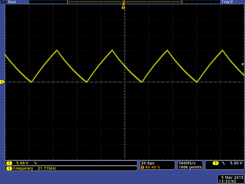
This is an interesting circuit with three voltage inputs, a constant multiplier, an index, and an offset. The crossfader is not a typical analog circuit. The two input signals are passed through CMOS switches which are alternately chopped at 21 KHz which is sufficiently high enough to not cause aliasing. The control adds an offset to the triangle waveform which effectively changes the duty cycle of the chopper. Think of this similar to a two channel scope in chop mode.
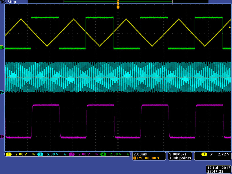
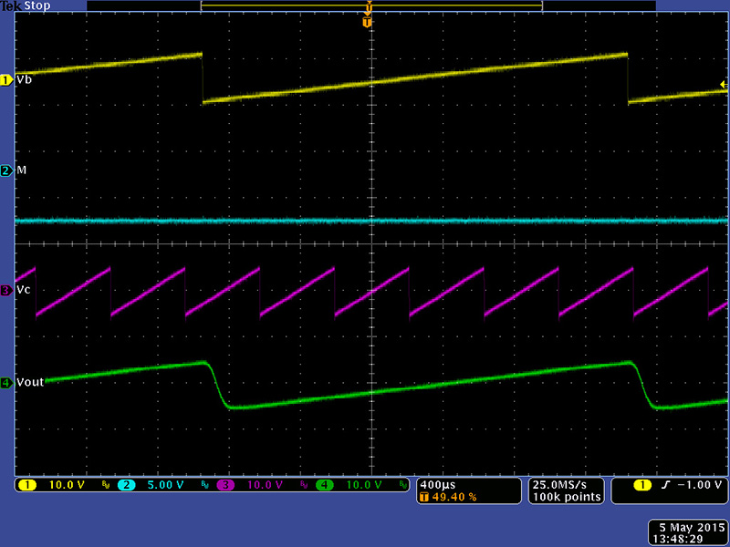
This image shows two inputs Vb (yellow) and Vc (green), the 21 KHz clock (cyan), and the output (magenta). This image is with the M control set to CCW to select Vb.
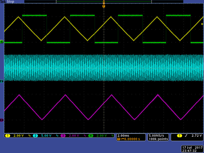
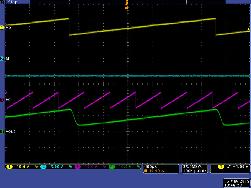
This image is with the M control set to CW to select Vc.
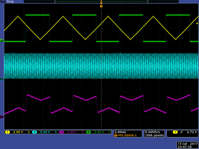
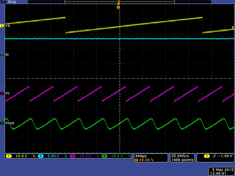
This image is with the M control set to mid position to select both Vb and Vc.
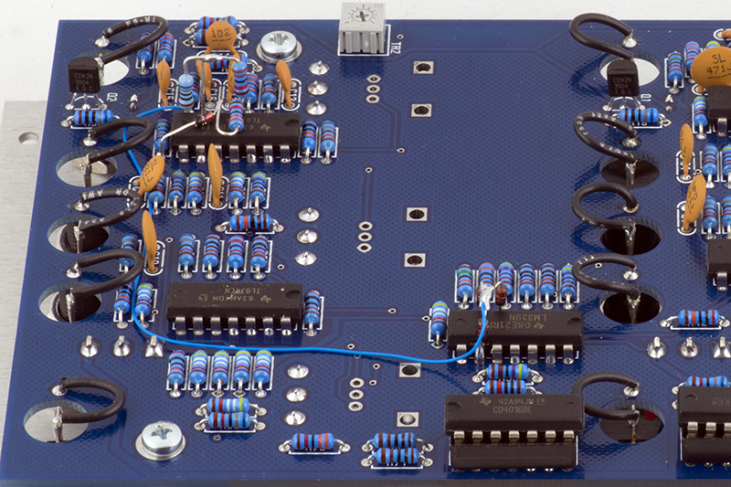
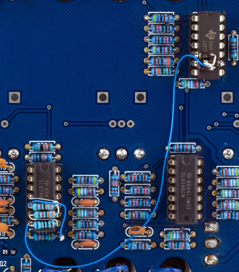
Initially my 21 KHz triangle wave did not oscillate. I discovered IC4 pin 14 was at -13V which reversed biased the input of IC2 pin 6. In looking at the circuit I discovered that the 0.2V clamp was not implemented as per the original schematic. This clamp would have kept IC2 pin 6 from becoming reversed biased. Below outlined in red is the original clamp circuit.
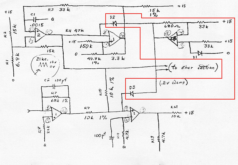
IC4 has one unused op-amp that is unused and not terminated so I decided to add the clamp modification.
The oscillator now runs at 21.7 KHz.
| 257 Clamp Modifications
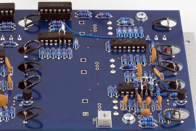
Everything on the original schematic in red needs to be added. The op amp in lower left is the spare op amp. Pin 4 is 15V and you can see connected to it are two 33K resistors (it is a TL074 so the pin numbers are different from the original schematic). You can see on resistor going to pin 5 and the other going to pin 6. The pin 5 also connects to the diode that goes to ground soldered at the resistor leg on the PCB. The 680R feedback resistor is connected between pins 6 and 7. Note that the vertical leads across the top actually descend and solder to pin 6. The horizontal leads descend and solder to pin 5. Then we wire over to the other op amp where we add 3 diodes. The cathodes of the diodes connect to the IC pins, and all the anodes are connected together. Here are two side photographs to help understand the modifications.
|
Calibration is straightforward. The trimmers set the center off position of the Va control. I simply put +5V into Va, set the Voffset to 0, and adjusted the trimmer so the output was 0V with the Va control centered.
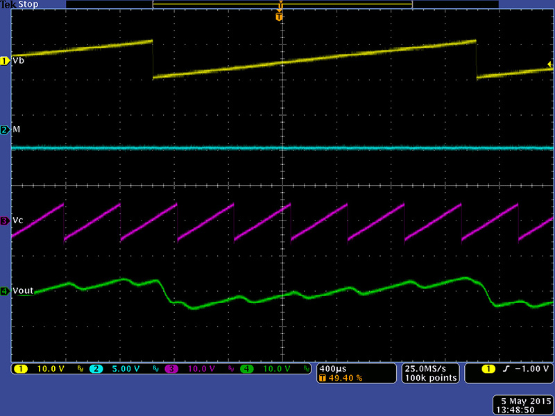
This image shows the voltage processing of two ramps. I have the M control set at center and have an external -5V into the M input. Vb is crossfaded to the output. I am not using Va as I don't have enough scope channels to display five signals.
This scope image shows the same setup with Voffset applied to shift the output positive.
Removing the Voffset and changing M to -5V crossfades Vc to the output. You can see distortion in the output waveform with a 2.5 KHz Vc.
An M index of -2.5V crossfades Vb and Vc together to the output.
Alternate Modification Technique
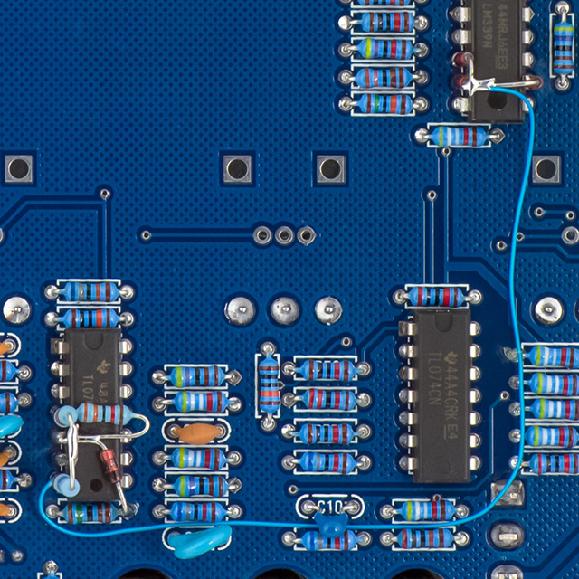
I have been making the modification with the parts standing up. They can be damaged if the module is set down on the back since those parts stick up above the others. I decided to make the modifications more secure with the parts laying flat as shown in this photo. One could also make the modifications on the rear of the PCB but often these modules come to me assembled.
To aid in the modification I have zipped together three good views of the flat parts modification. The short wire goes to a diode standing vertically with the cathode to the PCB. It is a bit hard to see in the photos.