 |
219 Compound Touch
Controlled |
|
I got the opportunity to repair a 219 that was likely built in the 1974 timeframe as the date codes on the ICs were 1973/4. This is quite a module with a little of everything. There was likely only a dozen of these ever produced.
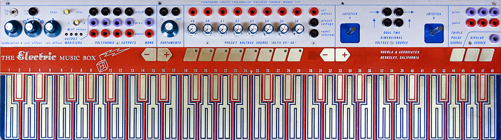
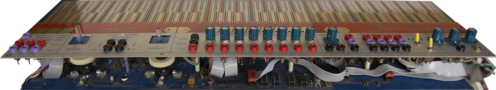
It has a 48 note polyphonic keyboard, Portamento, 8 pad preset voltage source, two joysticks, a triple pulse source, and one +/- voltage source with parallel pads.
The 48 keys produce the standard pulse, pressure, and CV output. They also drive a 4 note polyphonic output where each key press is assigned to one of four outputs, similar to the 264 module. LEDs indicate which channel the current key is assigned to. The polyphonic function can be set to 2, 3, or 4 outputs. There is a tune control to fine tune the CV output, an audio modulation input and control, and a CV modulation input and attenuverter control. Portamento is a separate section with its own input and output jacks.
There is an 8 pad preset voltage section with LEDs. Each pad has an individual pulse output and two common CV outputs, one for an equal voltage output and the other for a preset control.
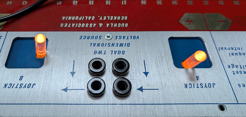
The two dimension voltage source joysticks look a bit wonky but function. They consist of a lamp and four LDRs with a shaft and shadow ring and have a ~ 13V range. The sticks also illuminate which is quite nice.
There is a 3 pad triple pulse source which provides separate pressure and pulse outputs.
Finally there is a bipolar source controlled by two parallel +/- pads. Think of this as a rudimentary mod wheel. When released the voltage goes to 0.
Construction
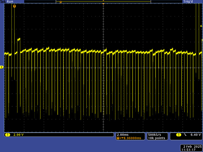
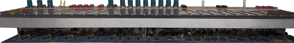
This module is a sandwich of various PCBs. The top two PCBs are for the pads. They are overlayed with an aluminum panel for the controls. Below are two circuit PCBs. One is for the key pad drivers. There are a total of 63 key pads so Don drove this as a 16 x 4 matrix. Each key has a trimmer that you set for equal amplitude. There is a separate trimmer to then set the overall level. I could adjust 62 of the keys correctly. There was one pad that wouldn't attenuate properly but connecting a probe would drop the level. I chose to leave this as it functions correctly. This module uses ribbon cable and is a bit fragile, and one has to move it around to make measurements and then test. It is a bit fragile so I wanted to handle it as little as possible. The tall spike is the unused 64th pad.
This is the module opened up for repairs and calibration. The PCB at the top consists of the trimmers and pad drivers. The bottom PCB contains all the circuitry and is mostly 4000 series CMOS so there are no rare parts in this module. You can see all the ribbon cable wiring. The gauge is small and the can break easily.
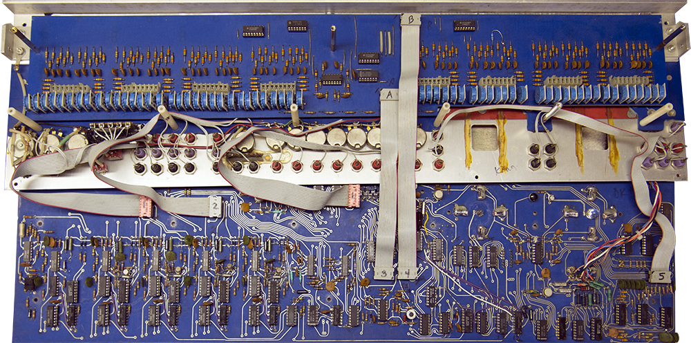
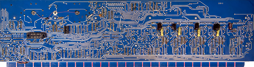
When assembled, the pad driver PCB is sandwiched in the middle. This image show the rear PCB and components from the front.
This image shows the rear PCB, components, and ribbon cables from the rear.
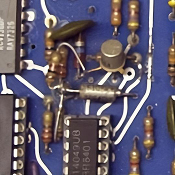
This image shows the rear PCB traces with a number of hand mods. The one incandescent lamp for the joystick had previously been replaced with a LED and resistor. The power connector was unused and wires soldered to the component side.
There are also a number of hand mods on the front of the PCB.
The joystick is an interesting design. The two incandescent lamps are driven from a circuit to ensure equal current at about 5V. The mechanism to block or pass the light is simply a Davies knob. A circular piece of PCB is attached at the top with a spring to close the panel opening.
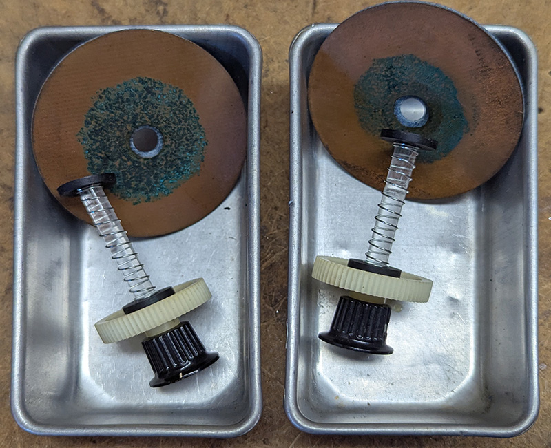
You can see three of the four CdS resistors around the lamp which forms the bottom pivot for the joystick.
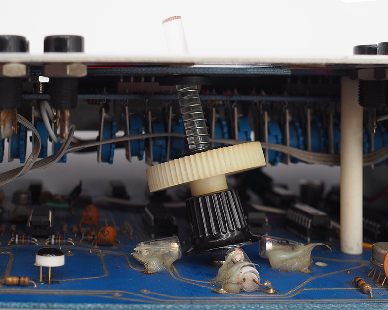
The joystick posts are clear and since centered on the lights illuminate for a nice touch.
I didn't take any additional operational images as these are standard Buchla pulse, pressure, and CV outputs. Besides, with something this rare I don't like to take any extra time to avoid any possibility of an accident.