|
111 Dual Ring Modulator Module |
|
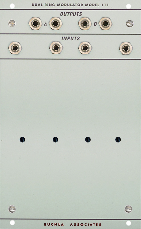
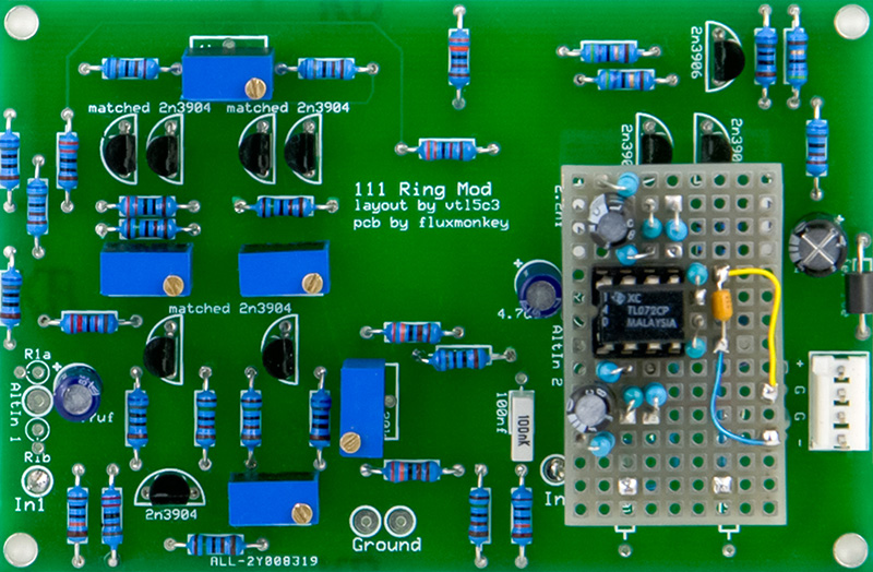
I've helped people build their Fluxmonkey 111 Ring Modulators but I have never had one to test and measure. Their calibration never seemed to work 100%, signal levels seemed to be off, and the modifications didn't make sense to me so I decided to evaluate it closer. This is a heavily Photoshoped panel image of a 111 Dual Ring Modulator module.
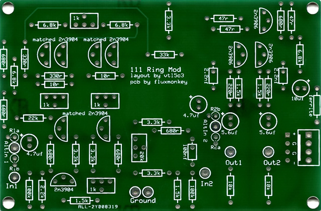
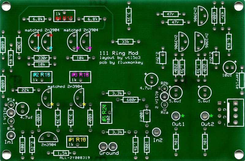
The Fluxmonkey PCB is for a single ring modulator so two need to be stacked to build a dual module.
The 111 design is very close to the circuitry used in the MC1496 Balanced Modulator.
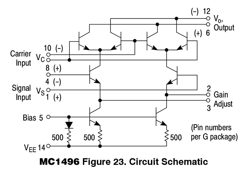
The schematic has a number of errors in it. Readily acknowledged is R37 and R89 should connect to +15V. R19 and R70 are shown on the schematic as 10R but I believe should be 10K as the two dual pairs should be identical circuits. R78 is thought to be 680K but 680R as per the schematic makes more sense feeding a 20K trimmer. In actuality I saw little difference between 680R and 680K.
111 Ring Modulator schematics (corrected)
I used cut tape transistor for both the 2N3904 and 2N3906 which has the advantage of matching Q1, Q2, Q3, and Q4. This image has my output level changes (see modifications below).
Calibration
There are several ways to calibrate the module but based on the schematic I chose to calibrate it as follows:. Q1 and Q2 have fixed bias via R5 and R6 as do Q3 and Q4. You need Q1, Q2, Q3, and Q4 to all be matched. R10 sets the balance between Q5 and Q6 so I trimmed these first. Adjust R10 for 0V between the emitters of Q5 and Q6 with no input signals.
Then set the balance between Q1 and Q2. Adjust R13 for 0V between the emitters of Q1 and Q2 with no input signals.
Then set the balance between Q3 and Q4. Adjust R18 for 0V between the emitters of Q3 and Q4 with no input signals.
Then set the balance between pairs Q1/Q2 and Q3/Q4. Adjust R17 for 0V difference between the collectors of Q1 and Q2 with no input signals.
In 2 sets the gain for these differential cells and is adjusted for minimal output with In 1 grounded. In 2 is AC coupled and C2 rolls off the low end so use a 1 KHz 4V pk-pk sine wave. Adjust R24 for minimum signal output on Out 1 and Out 2.
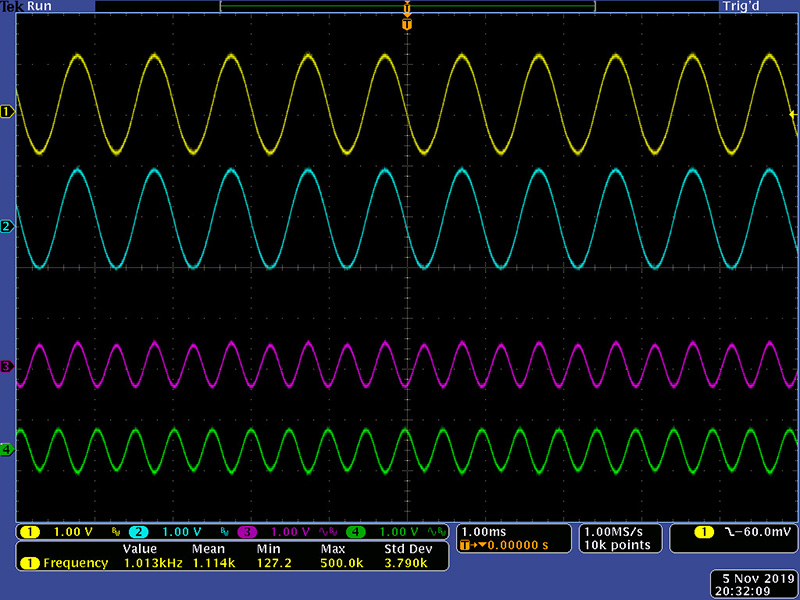
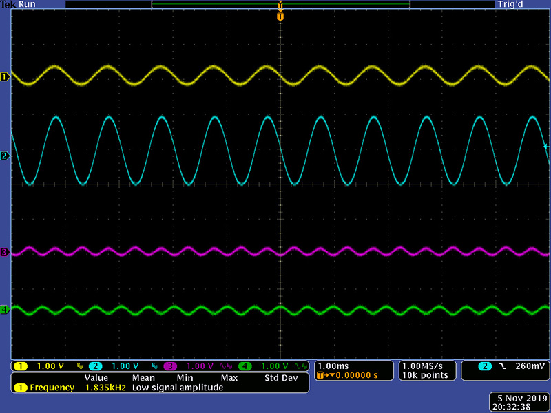
This image shows a 2V pk-pk 1 KHz sine on In 2 (cyan). In 1 (yellow) is floating and there is signal bleed which affects the calibration.
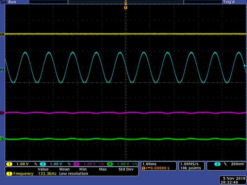
This image shows a 2V pk-pk 1 KHz sine on In 2 (cyan). In 1 (yellow) is grounded and the outputs can be trimmed to near 0..
This image shows the trimmers, steps, and measurement points.
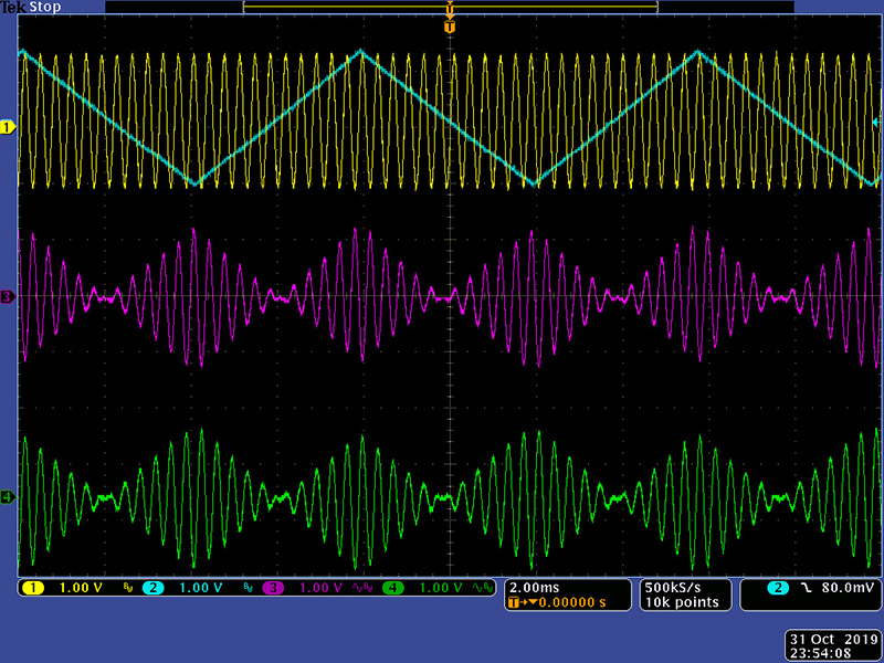
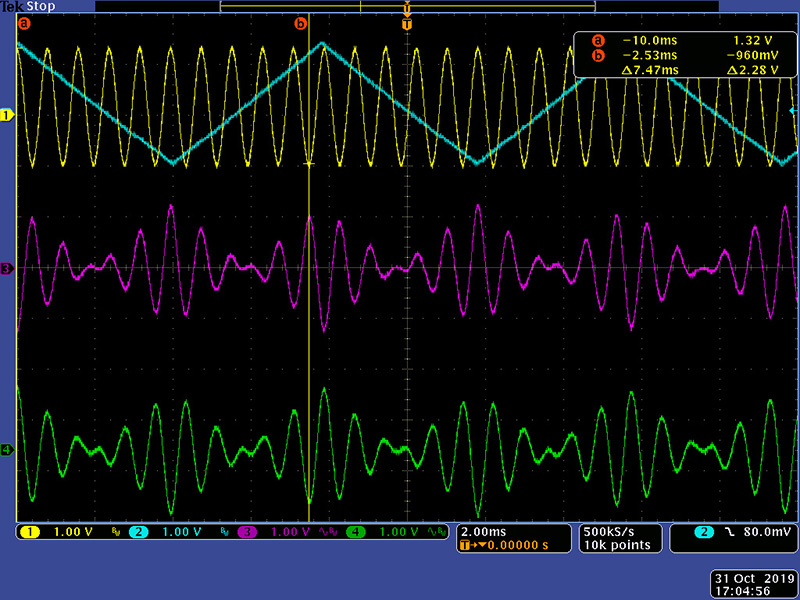
Now apply signals to Ch 1 and Ch 2. I used a 100 Hz 4V pk-pk triangle wave for Ch 1 and a 1 KHz 4V pk-pk sine for Ch 2. Note the amplitude of the outputs are only about 200 mV pk-pk. These images show my my higher output levels (see modifications below).
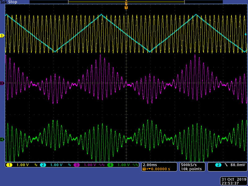
Adjust either (but not both) R13 or R18 for symmetry about ground in the envelopes. Note the envelopes may not be the same amplitude.
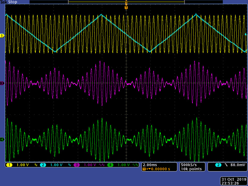
Now adjust R10 so the envelopes have the same amplitude. I found R10 had very little affect (see modifications below).
Modifications
I changed R14 and R19 to 1K5 to give about 50% more gain which brought the outputs up to about 300 mV pk-pk. I changed R9 and R11 to 1K5 to give more trimming range to R10. I tried adjusting the output gain but ran into distortion and bias issues. It was easier and simpler to add a single- supply dual op-amp with a gain of 7.8X to bring the output levels up.
111 Ring Modulator modifications
Operation
Lowering the frequency you can see that the two outputs are opposite phase.
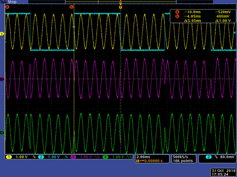
A square wave signal reverses the phase of the carrier in balanced/ring modulator.
Using the same signal on both In 1 and In 2 results in a frequency doubling.