 |
Serge Modular
Rebuild |
|
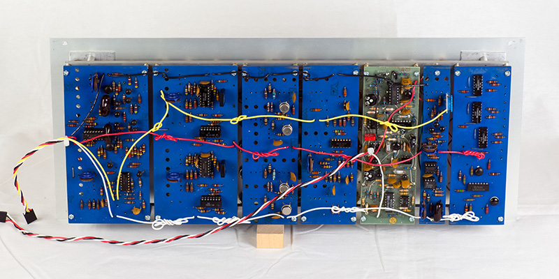
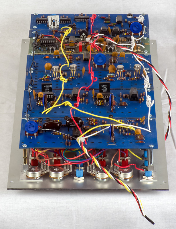
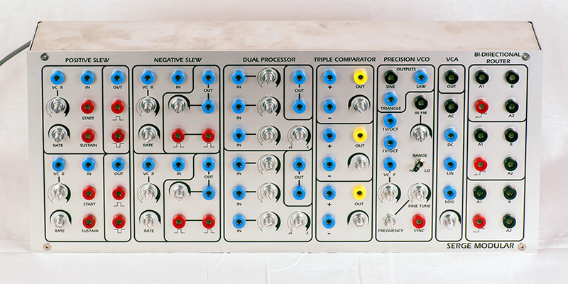
Box 1 consists of a R10 Positive Slew, R9 Negative Slew, R1 Dual Processor, R11 Triple Comparator, 106B Precision VCO, R6 Gate (VCA), and a R4 Bi-Directional Router.
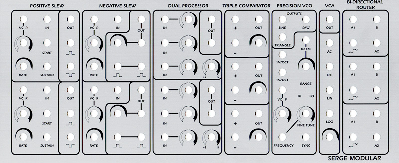
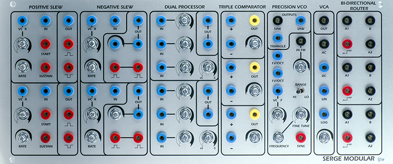
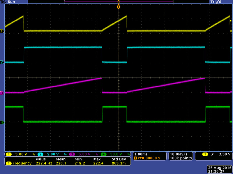
R10 Dual Positive Slew
The Positive Slew has Start and Sustain inputs for more control than the Negative Slew. If you cross-wire Start and Negative Pulse between the two halves you create a VCO with minimum frequency of 0.8 Hz and maximum frequency of 1800 Hz. This scope image shows the two slew outputs and the two positive pulse outputs.
R9 Dual Negative Slew
The panel for this Negative Slew has output attenuators that I added.

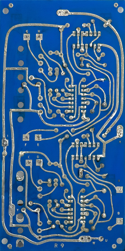
R1 Dual Processor
The Offset control for this processor only provided 0 to +5V offset. I rewired the Offset control with +/-12V so it would offset +/-5V. With the design and resistor tolerances none of the channels provided unity gain but they were close.
R11 Triple Comparator
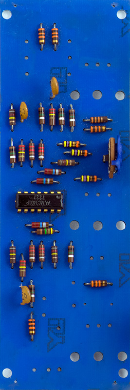
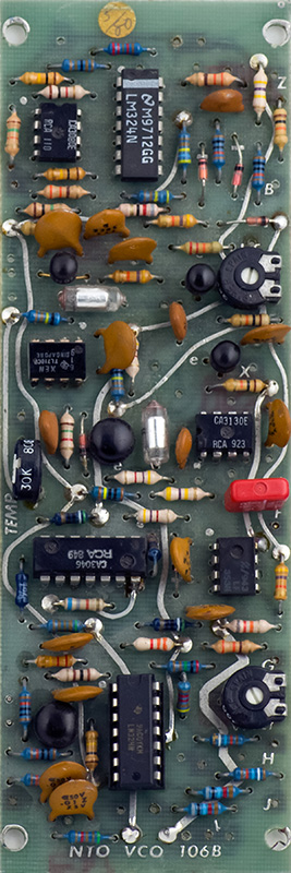
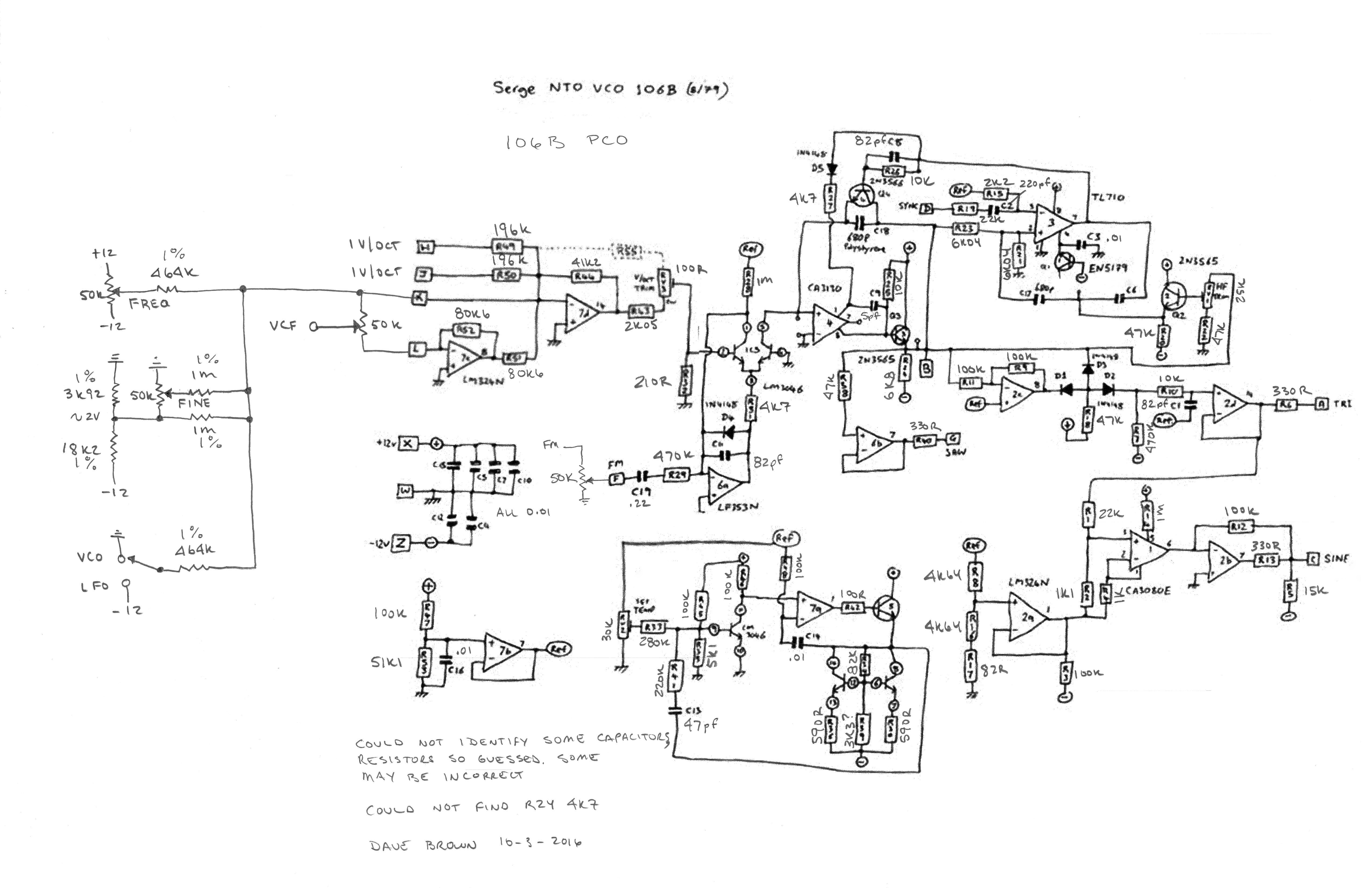
106B PCO VCO
I added the front panel parts on the schematic and also the resistor and capacitor values. Some of the legends on the original schematic are not legible so I did my best guess for for the values of those parts. Some may be incorrect but it helped me figure out the front panel wiring.
The TL710 has an interesting negative supply. It is connected through a reversed BE junction of a EN5179 transistor. The TL710 has a maximum voltage rating of -7V and is powered from -12V so they must be using this transistor as a zener diode. I can't find a datasheet for a EN5179 but the PN5179 has an emitter-base breakdown voltage of 2.5V minimum, so that isn't enough of a voltage drop. Maybe they hand selected parts or maybe the EN5179 had a higher breakdown. The interesting question is why didn't they just use a zener diode?
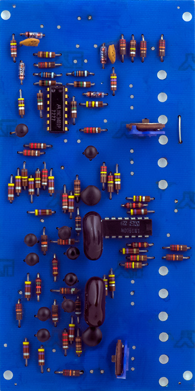
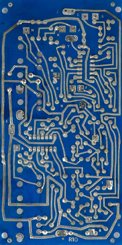
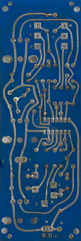
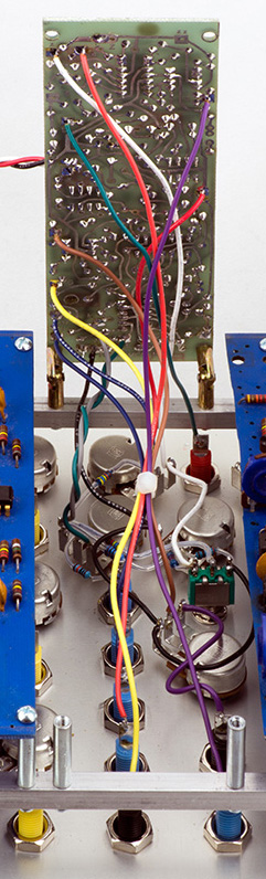
This image shows the 106B PCB rotated up. The 106B has the most complex panel wiring with 6 resistors and the range switch. I chose to connect the panel +/-12V to the PCB and route the 106B power wiring separate from the other modules for isolation. I do believe the wiring diagram for this is wrong with Sine and Saw (C and G) swapped. The lower yellow and violet wires had to be swapped after this photo was taken.
The Triangle and Ramp outputs are 4V unipolar and the Sine wave is +/-2V bipolar. The 106B has a frequency range from 0.7 Hz to 585 Hz in the Lo range. The waveform at the lowest frequency is very nicely shaped.

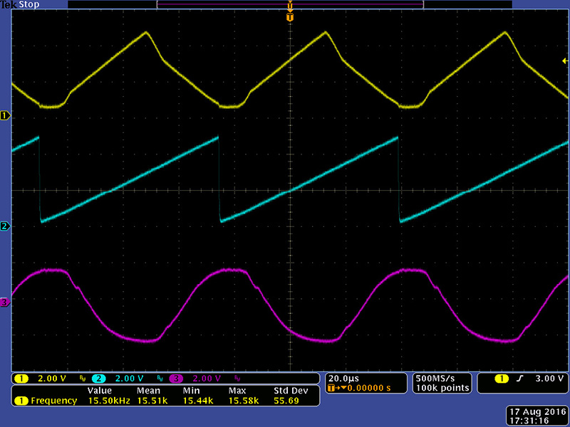
The 106B has a frequency range from 17 Hz to 15.5 KHz in the Hi range. The waveforms have some distortion at 15.5KHz.
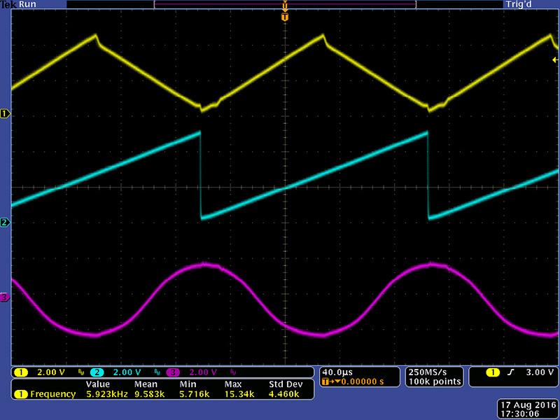
At 6 KHz the sine waveform looks pretty good but there is still a bit of mismatch at the triangle peaks. There is no trimmer to adjust this.
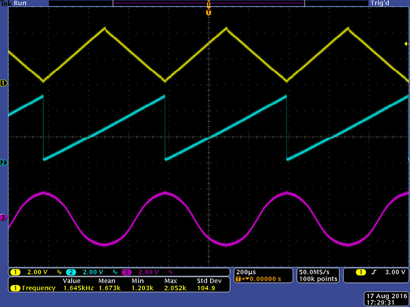
At 1.6 KHz the waveforms look very nice and the mismatch at the triangle peaks is pretty minimal.
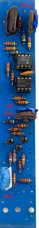
R6 Gate (VCA)
This scope image shows linear operation of the VCA with a 5V control signal.
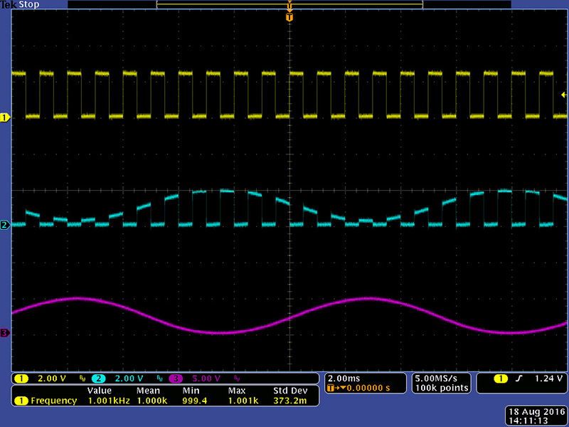
This scope image shows log operation of the VCA with the same 5V control signal and the Gain control set to 9 O'clock.

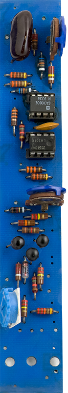
There are several different schematics for the R6 Gate all with minor differences. The only accurate schematic I found was at serge.synth.net. Note that X and Y are mislabeled on the PCB which swaps +12V and +6V. With the wrong supplies it still operates but requires 10V control signals. I noted the correct X and Y pads on the PCB image.
I calibrated the VCA by turning the gain control fully CW and adjusting the Gain trimmer for unity gain. I then removed the input signal and adjusted Offset for 0V DC on the output. The kit instructions say full gain when using the log input is with the gain control at 9 O'clock so I set it there and adjusted the Log Gain for unity output with a 5V control signal.
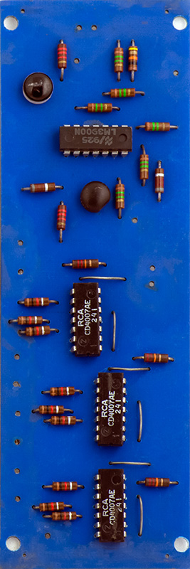
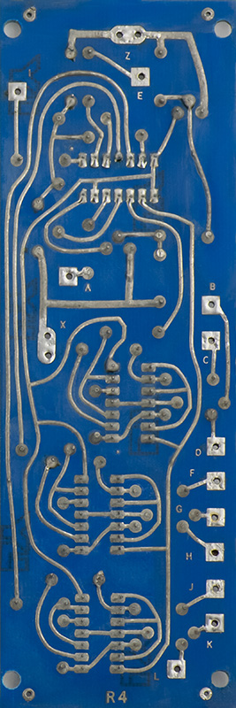
R4 Triple Bi-Directional Router
Construction
A bus bar mounted on rear brackets holds all the PCBs which hinge from the bottom. The power is daisy chained between all the modules except for the VCO which has a dedicated power cable. The twists in the power wires is to allow slack for the PCB to be rotated up.
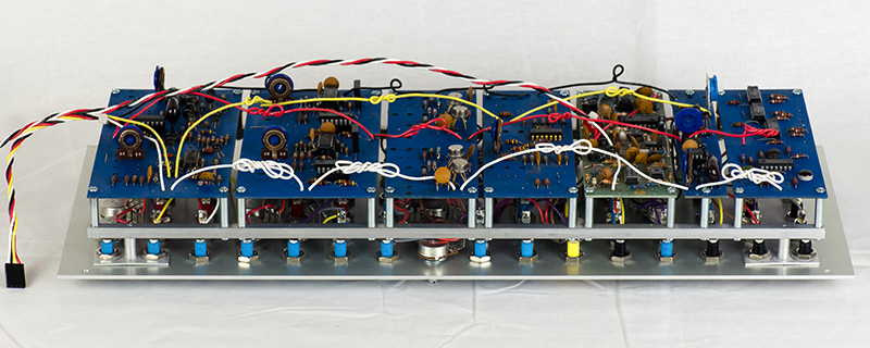
This side image shows the hinged standoffs and the panel wiring.
The box is quite clean with only 4 panel screws in the front.
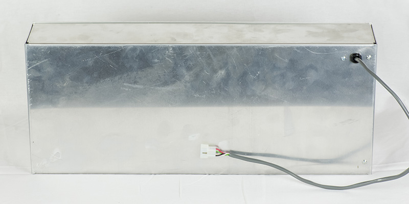
The rear just has the Serge 4 pin connector for power.