|
266 Source Of
Uncertainty |
|
I have the V1.1 PCBs. There is just enough room at the THRU pads to add a 0.1" MTA connectors I can run a power cable to PCB 2.
The stored random voltages Stp Out (Out 1) is 0 to +10 volts and are discrete but not quantized to semitones. The CMOS logic in this circuit is operated on +10V so input protection is required from the op-amp comparators since it swings from rail to rail. The original protection circuitry consists of a series resistor/divider to limit the current and rely upon the over and under voltage protection diodes in the 4000 series CMOS. I find 4000 series CMOS fragile enough so I modified the circuit with schottky over and under voltage protection. I made modifications for 5V CV input and 5V outputs.
The CV integrator is a straightforward design and is setup for a 12V control and 10V CV. I made modifications for +15V control and 5V CV input.
The sample & hold is an interesting setup. There is a divide by two on the input pulse which creates two alternating output pulses for the two S&H's individual outputs which are bipolar. These outputs are also multiplexed together to form a single S&H output that is only positive voltages. The input and output pulses are setup for 10V so I made modifications for 5V input pulse, improved negative input protection, and 5V output pulses. The CMOS in this circuit is operated on +15V so only negative input protection is required. The outputs track while the sample clock is high so I shortened it from 3 mS down to around 150 uS.
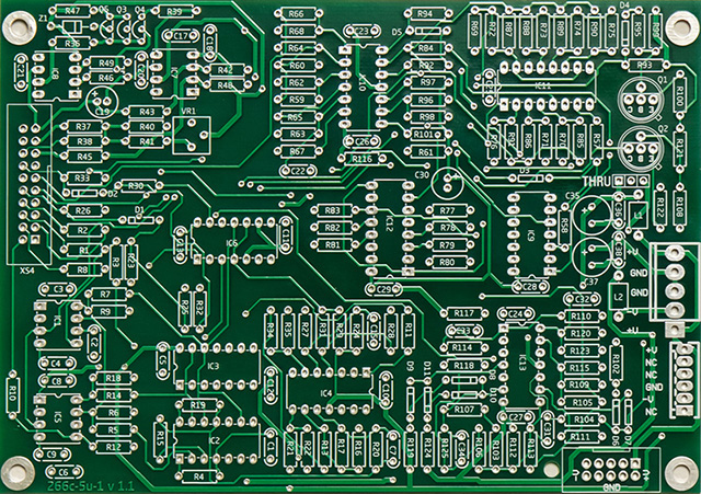
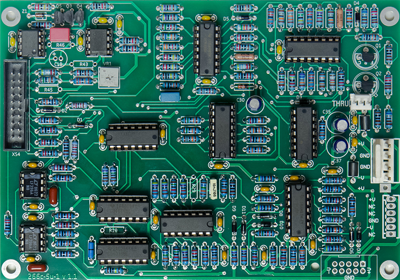
PCB 1 Modifications: (Note: applies to the 266c-5U-1 v1.1 board)
Integrator
Sample & Hold
Stored Random Voltages
|
VC Integrator schematic modifications (topology change schematics at bottom of this page)
Sample & Hold schematic modifications
PCB 1 Mouser Excel BOM updated
PCB 1 power consumption measurement: +15 @ 42 mA, -15V @ 40 mA (no LEDs)
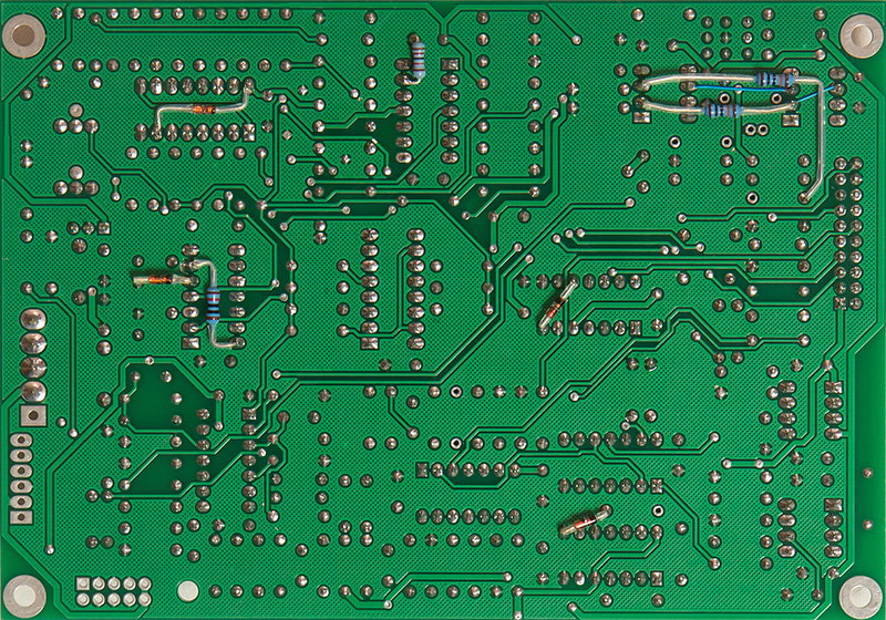
This PCB has the integrator topology changes which are documented towards the bottom of this page. The only cut runs are the ground traces around IC9 pin 9.
The integrator topology changes are the two resistors and two wires in the upper right corner. The other additional parts are the CMOS protection diodes, pullup resistor, and 5V output mod resistor.
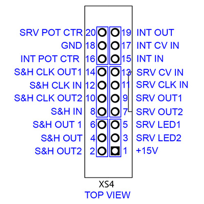
3x1 and 4x1 FCI mini-latch connectors fit inside the XS4 ribbon connector header to connect the front panel wiring.
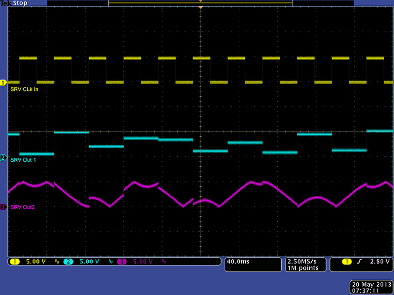
SRV Operation
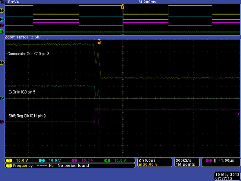
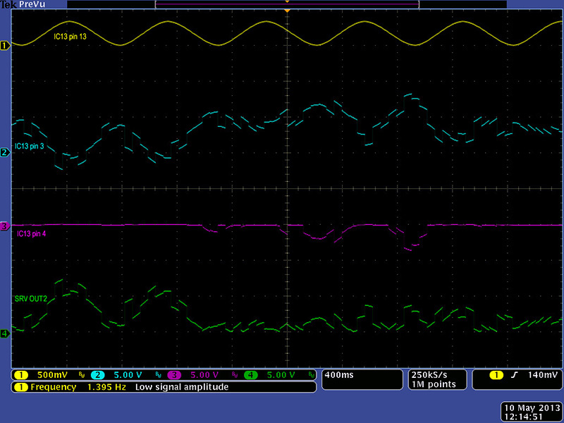
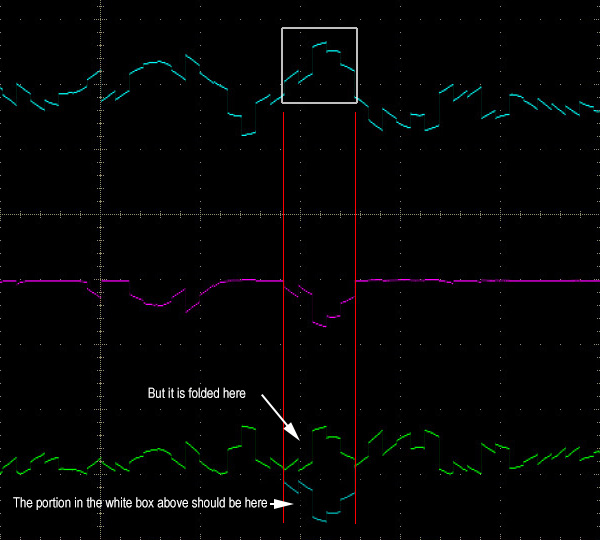
I could see the outputs of the shift register changing on the falling edge of the input pulse and hear the output change on the half-step. I found the input op-amp used as a comparator didn't have enough hysteresis to filter out the glitches from my 566 VCO (I didn't know my 566 VCO outputs had glitches until I looked at the SRV). I played with the hysteresis level and added a 2N2 filter capacitor across R68 but decided to leave the circuit as-is and use a better clock input as from my Wogglebug module. In this scope image you can see the op-amp comparator output glitch propagate through to an extra shift register clock.
Both SRV outputs are quantized (e.g. discrete) voltage steps, but not quantized to any particular V/Oct scale. Also note that the CMOS logic outputs will not drive to 0V so there is a minimum voltage offset. The SRV produces pseudo-random voltages in discrete steps but not musically scaled steps.
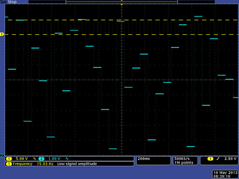
SRV Stp Out (Out1) is an 8 bit binary weighted resistor ladder that divides the 10V into 255 steps of 39.2 mV each. The Vol of the CMOS shift register measured 371 mV and the Voh measured 10V so the actual steps are a bit smaller.
This scope image shows the SRV Stp Out.
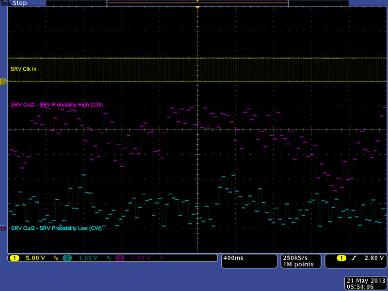
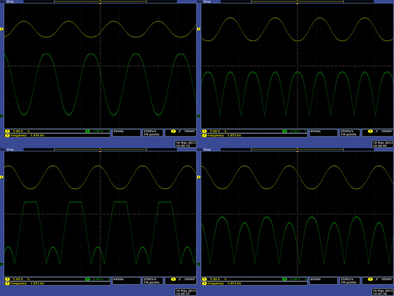
SRV Sum Out (Out2) has a 15 bit resistor ladder resistor divided into three groups of five different resistor values distributed randomly throughout the 15 bits. The 200K resistors contribute 0.5V/bit, the 180K resistors contribute 0.556V/bit, the 150K resistors contribute 0.667V/bit, the 130K resistors contribute 0.769V/bit and the 120K resistors contribute 0.833V/bit. The voltage from this resistor ladder is summed with a CV probability control and external CV input, is shifted and can clip, and is processed by a non-linear stage (I have never seen a good description of what the non-linear function is). The probability control level weights the output towards the high or low portion of the 0 - 10V output region. These two scope images were superimposed to see the effect of the probability control (note I have converted the output to a 5V range for this image).
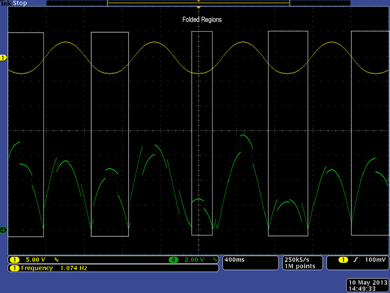
The interesting part of this circuit is the weighting to the higher or lower voltages but still remaining within in the 0 - 10V range. The non-linear processing is a wavefolder set at +/- 4.8V (e.g. ~10V range) and the shifted waveform is simply folded back at 0 and 10V. These next scope images show the wavefolding in more detail. This scope image shows the signal path from the SRV CV In sine wave (yellow), the shifted and inverted sum of the SRV CV In, probability control, and the pseudo-random outputs (cyan), and the wavefolder inverted peak detector (magenta) which is subtracted at 2X gain to fold the peaks so that SRV Out2 (green) remains in the 0 to 10V range.
This superimposed image shows how the peak is folded. The wavefolding circuit is an interesting design. R119 and R124 set the current through the diode bridge. The diode bridge is biased and effectively shorts the output to the negative input keeping the op amp output at 0 volts. As current is injected into the bridge through by R107 the diodes rebalance the current keeping the bridge biased. However, when the current through R107 exceeds the the current through R119 or R124 it unbiases the diode bridge and the op amp forms an inverter with a gain of -1 as determined by R125/R107. The threshold is set at +/-4.8V by the ratio of R107 to R119 and R124. The output stays at 0 volts until the input exceeds +/-4.8 V as seen in the magenta trace. This peak is added at 2X gain to the original signal to fold the peaks back. The level shifting is setup appropriately so that the sum of the pseudo-random resistors and the SRV CV is always in the 0 to +10V range. Neat!
Here are a couple of more examples of the wavefolding. I ran the SRV clock until I got a particular wavefolding and then stopped the clock. You can see the resulting SRV Sum Out range from no folding to complete symmetrical folding and various partial foldings in-between depending on the DC level shift from the shift register outputs.
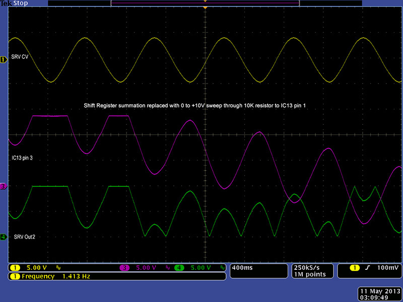
The 15 resistors on the output of the shift registers provide a voltage range of 0 to 10 V through an equivalent 10K series resistor. For a more precise look at the wavefolder operation I removed the shift registers and injected a 0 to +10V sweep through a 10K resistor to pin 1 of IC13. You can see the level shift, clipping, and wavefolding of the SRV CV in this scope image.
You can see the significant wavefolding folding with a large SRV CV input.
I prefer an output voltage in the range of 0 to +5 volts so I changed both SRV outputs to 0 to +5V as seen in this scope image.
Sample & Hold
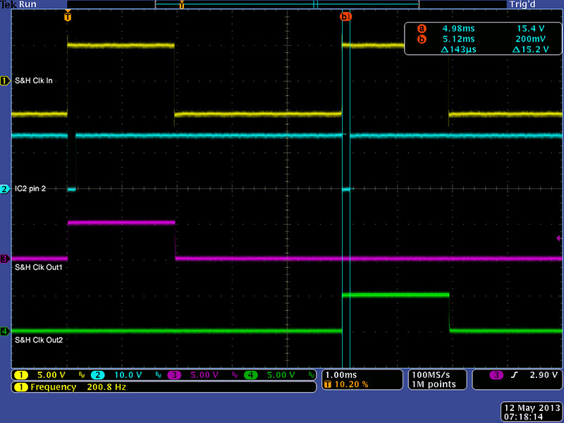
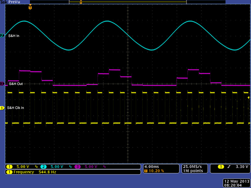
I modified the S&H Clk In circuit with the same modifications as the SRV Clk so it operates on 5V signals with CMOS protection for negative voltages. This scope image shows the S&H Clk In signal generating the S&H pulse and the two 5V S&H Clk Out1 and Out2. The S&H tracks while the sample pulse is true so I shortened it to 140 uS.
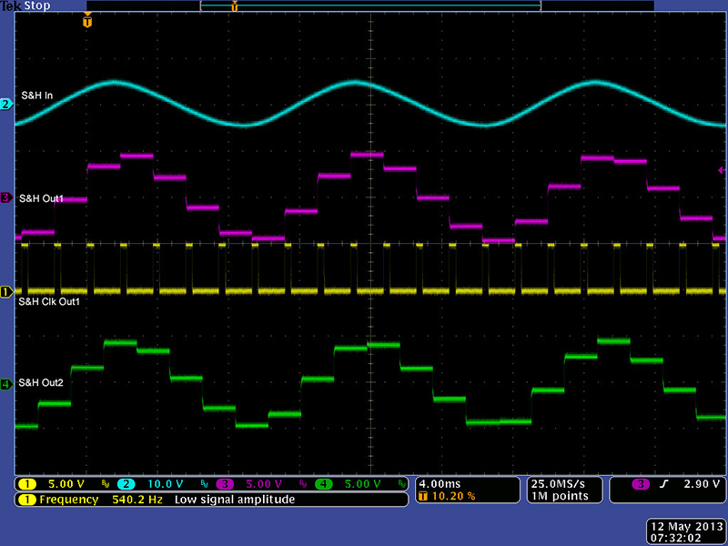
This scope image shows S&H Clk Out1 which is half the frequency of the S&H Clk In signal. You can see it sample the S&H In on the rising edge of the clock. You can also see how S&H Out2 is changing half way through the cycle on the alternate phase S&H Clk Out2. Both S&H Out1 and S&H Out2 are bipolar.
S&H Out is the combination of only the positive portion of S&H Out1 and S&H Out2. You can see where it samples on every rising edge of the S&H Clk In. Why you would only want the positive portion is a bit of a mystery to me. One would have to change the CD4016 to a +/-15V compatible part to have a bipolar output.
CV Integrator
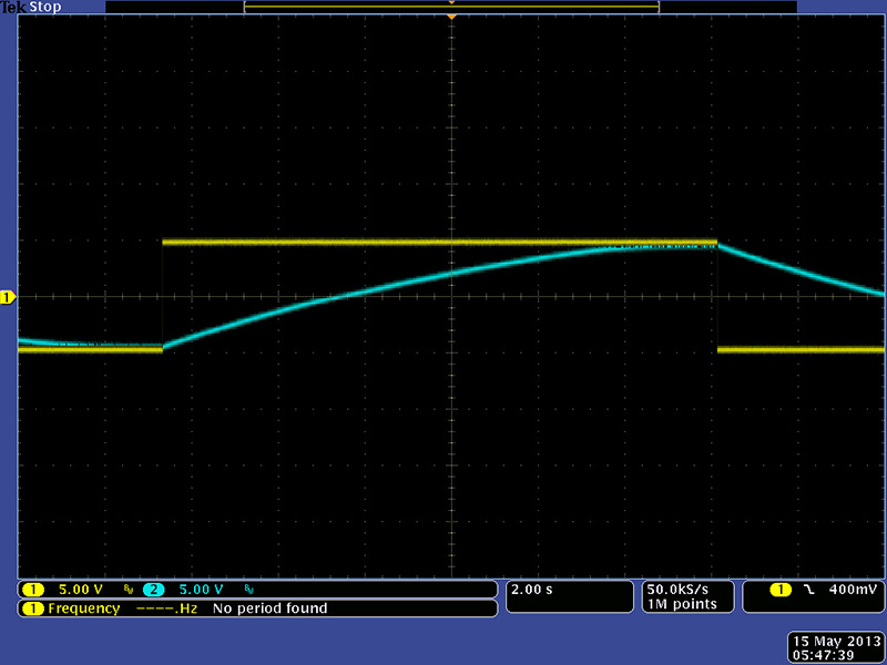
The integrator will operate on both positive and negative inputs. C19 should be changed to a non-polar capacitor if the integrator is to be used with negative input voltages. VR1 adjusts the minimum and maximum times for the integrator (CCW is shorter and CW is longer). Using just the front panel control with no CV input and VR1 adjusted full CCW the minimum integration time over 10V was 5.58 mS (1.79 V/mS) and the longest was 493 mS (0.02V/mS).
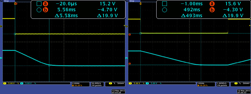
Adjusting VR1 full CW the minimum integration time over 10V was 21.3 mS (0.47 V/mS) and the longest was 32.9 seconds (300 µV/mS). I adjusted VR1 so that my maximum integration time was 10 seconds (1 mV/mS, or 1V/S).
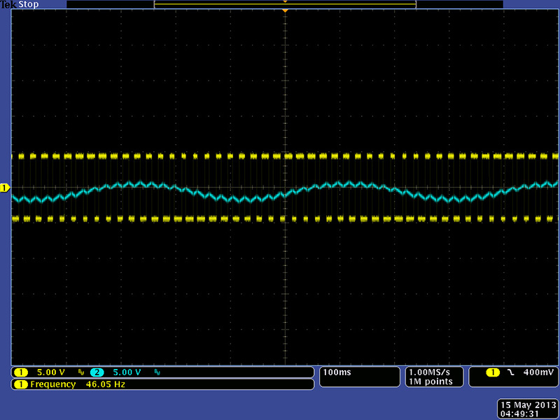
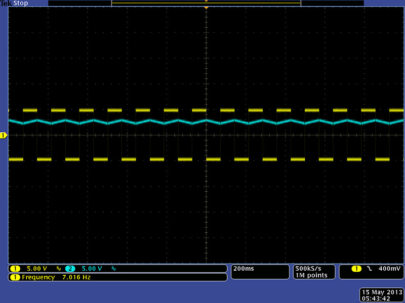
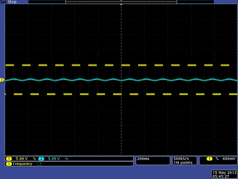
I ran my LFO square wave output through a divide-by-two to make sure it was a 50% duty cycle since this affects the integrator output DC level. There is no DC reference for the integrator capacitor so operation with a faster clock input than the integration time will cause the DC level to drift as shown in this scope image.
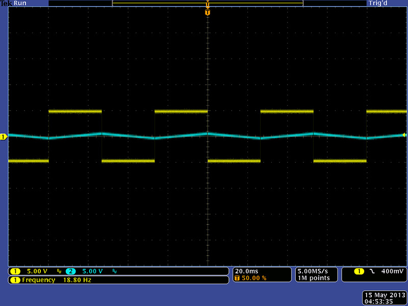
Adding a 10M resistor across C19 provides a fixed gain for the DC offsets so minimizes the drift significantly as seen in this scope image.
Unfortunately adding the 10M resistor to correct the DC drift makes the output non-linear although it is only really noticeable at long time constants.
CV Topology Modifications
I decided to change the topology of the integrator by moving C19 to ground and buffering it with a voltage follower to eliminate the drift and non-linear issues. Unfortunately the inputs to the CA3080 have to be reversed but can be done so by swapping the input from R43/R42 to R45/R48. These changes are fairly easy to make on the PCB.
PCB 1 Modifications: (Note: applies to the 266c-5U-1 v1.1 board)
Integrator Topology Changes
|
VC Integrator topology change schematic modifications (changes the integrator topology for improved DC performance)
I ran my LFO square wave output through a divide-by-two to make sure it was a 50% duty cycle and you can see the no-drift linear output in this scope image.
The input duty cycle of the input changes the DC level of the integrator when the input period is much greater than the integrator time constant. I changed the setup to slowly modulate the input duty cycle and you can see the DC level follow the modulation in this scope image.