 |
245
Sequential Voltage |
|
I built a 245 Sequential Voltage Source module for someone else. They sent me a complete kit of parts and I assembled and tested the module. Many of the components are sourced through Mouser but specialized parts, panel, and knobs have specific sourcing requirements. PCB1 has SPDT switches for Start and Stop with LEDs above them. The panel had holes for illuminated SPST switches so I had to use panel mounted switches and left the LEDs off. I couldn't find small SPDT switches so had to modify the Stop circuit for a SPST switch by grounding IC5 pin 12 and adding a 1 uF capacitor across the Stop switch to debounce it, and grounding IC5 pin 12 (SW1 bottom pad).
There is no power-on reset. At power up the pulser may be on or off. If off, any of the 5 stages can be on. I thought mine had failed since I had stage 5 disabled and it powered up on stage 5. Obviously when you start the pulser nothing happened.
On power up the pulser may be started or stopped and any of the stages may be selected. I see nothing in the schematics to power up the 245 in a known state so I believe it is inherent in the design. While possible to add circuitry to do so, it seems reasonable to initialize the 245 with the switches.
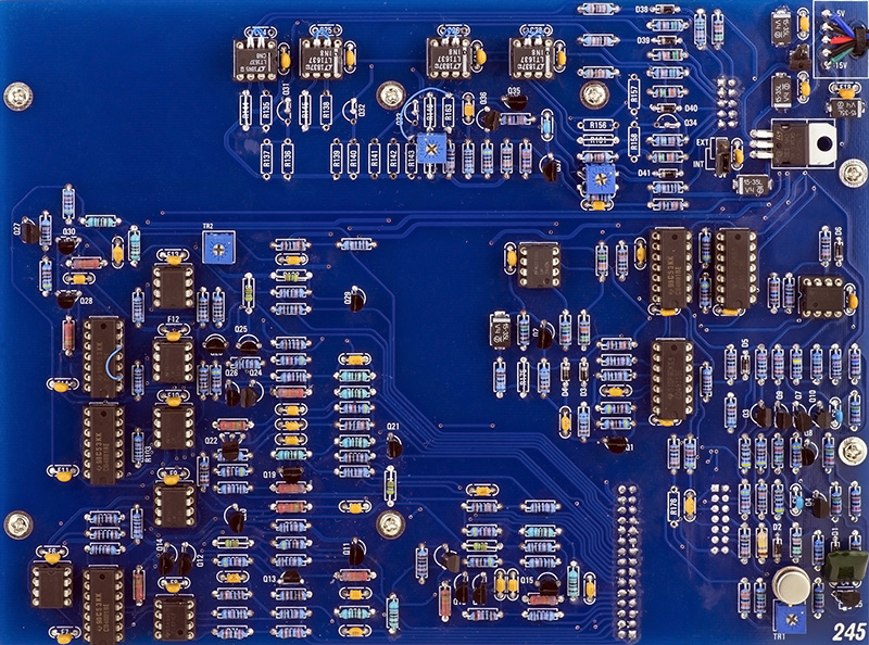
PCB1 has a few discrete parts but is mostly the potentiometers. You can see in this image SW1, SW2, LED1 and LED2 are not installed.
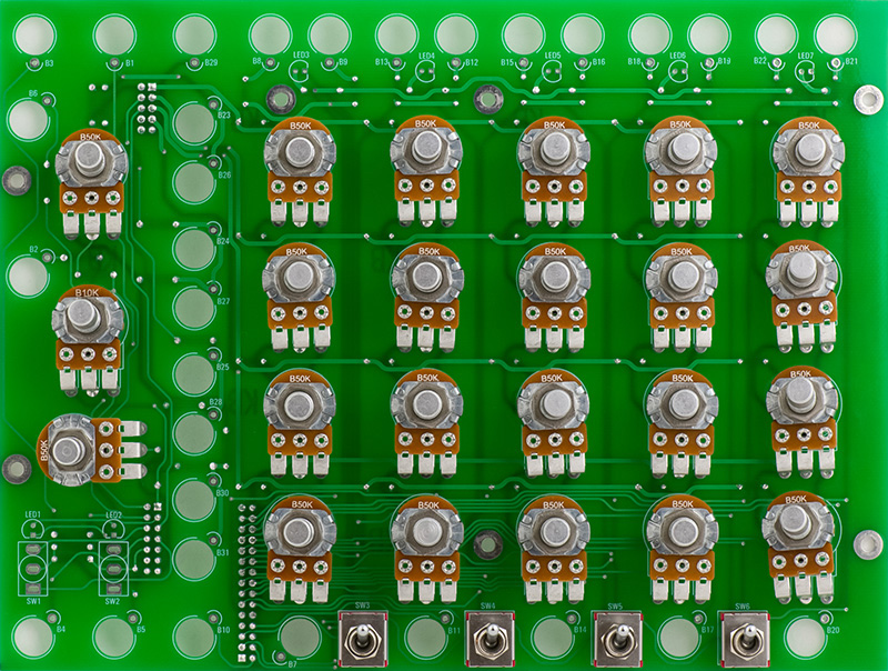
The discrete components are all mounted on the rear. You can see the wires from the panel mounted switches connecting to SW1 and SW2 and the Stop debounce capacitor in the lower right corner.
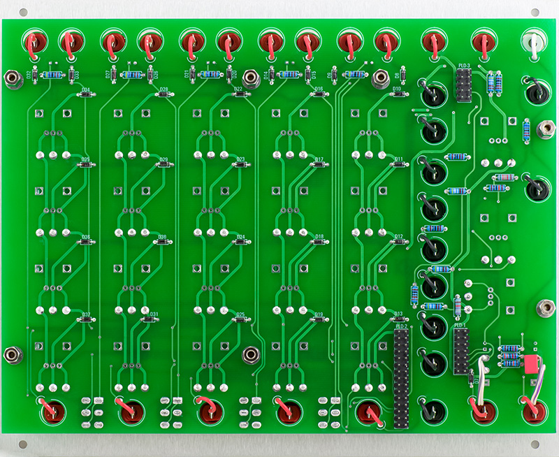
The front of PCB2 is just the board-to-board interconnects.
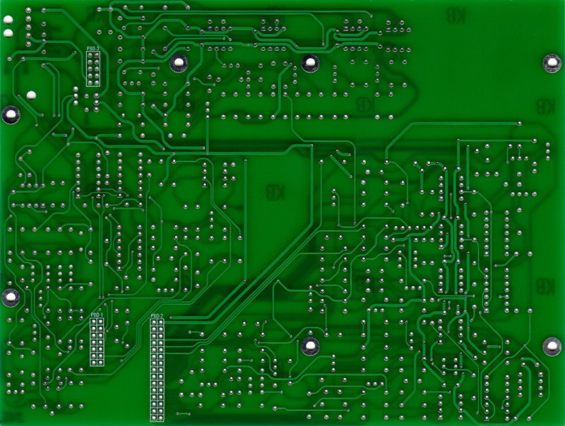
The components are on the rear of PCB2.
I made reference designators from the PCB images. The components cover the silk screen legends once populated which makes it hard to debug if anything is wrong.
PCB1 Front Reference Designators
PCB1 Rear Reference Designators
PCB2 Front Reference Designators
PCB2 Rear Reference Designators
Operation
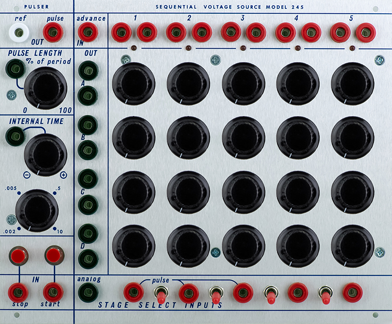
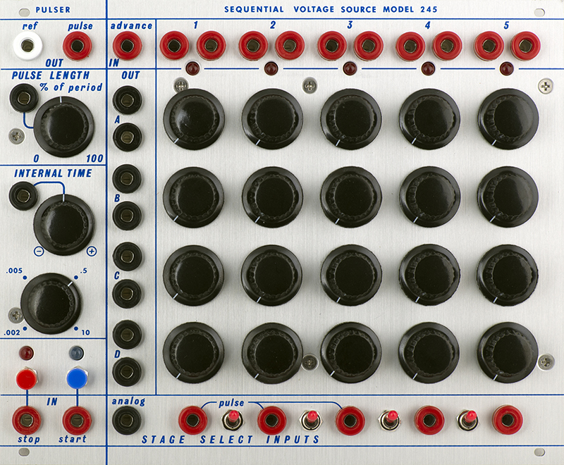
There is very little documentation on the245. It is comprised of two separate sections: Pulser and Sequencer. The Pulse output must be patched to the Advanced jack in order to operate. Start and Stop are self-evident but releasing stop advances to the next stage. This allows you to manually advance the sequencer with the stop button.
The outputs across the top are pairs of gate outputs indicating when that stage is selected. The inputs across the bottom select the stage. If you have the stage switches set for a Stage1-Stage2 sequence and pulse the Stage 3 input then the sequencer will begin a Stage3-Stage-4-Stage5 sequence so you can "flip" between sequences. The Analog input is a VC control to select a stage.
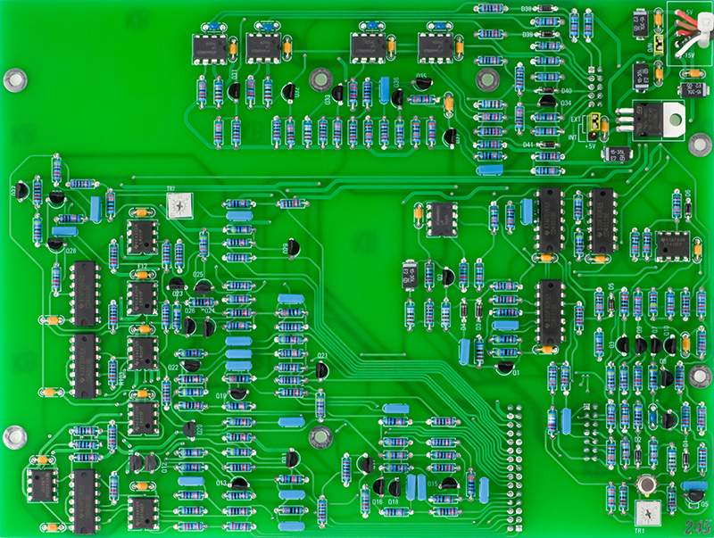
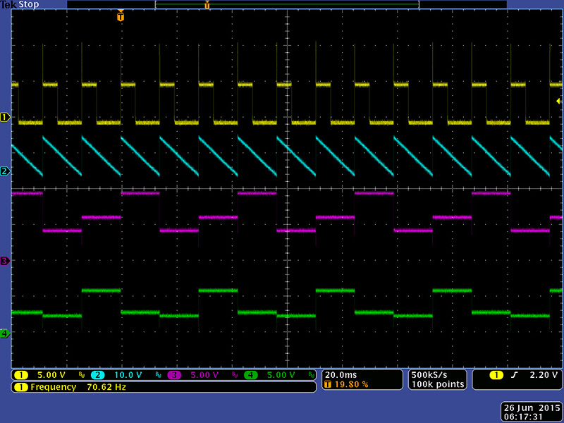
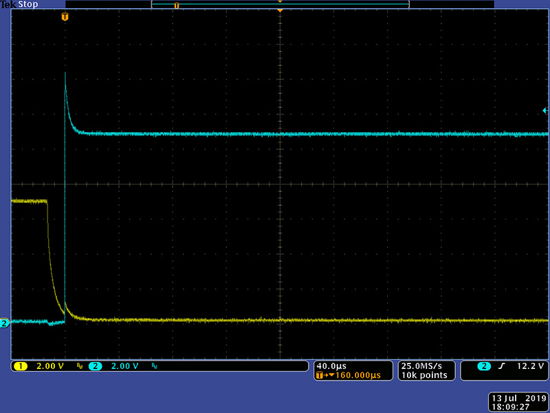
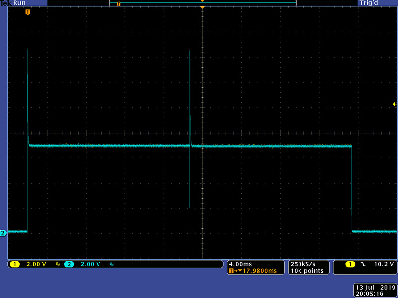
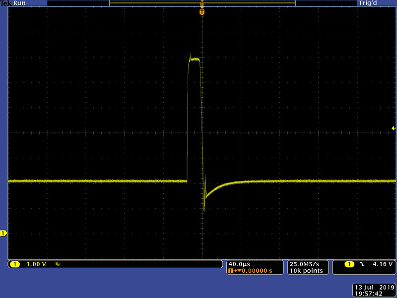
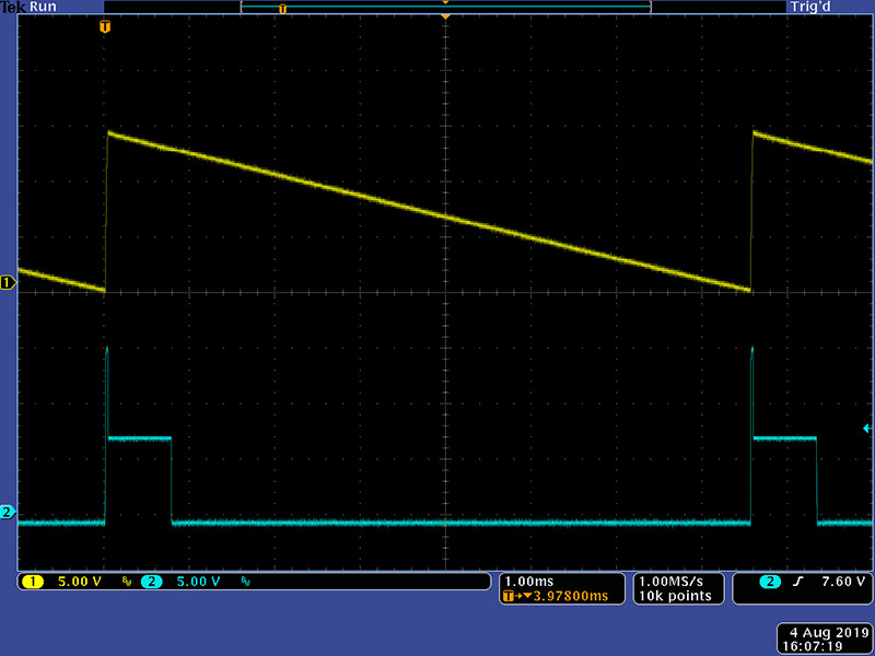
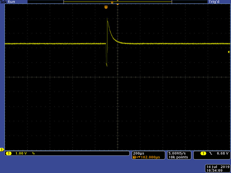
This scope image shows the pulse which is a combined trigger and gate at the minimum pulse length.
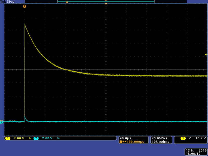
The Pulse Length control sets the width of the gate portion as seen in this scope image.
The Reference is a Saw output of the Pulser. The internal time modulation will pickup noise and should be set to center when the external input is not used.
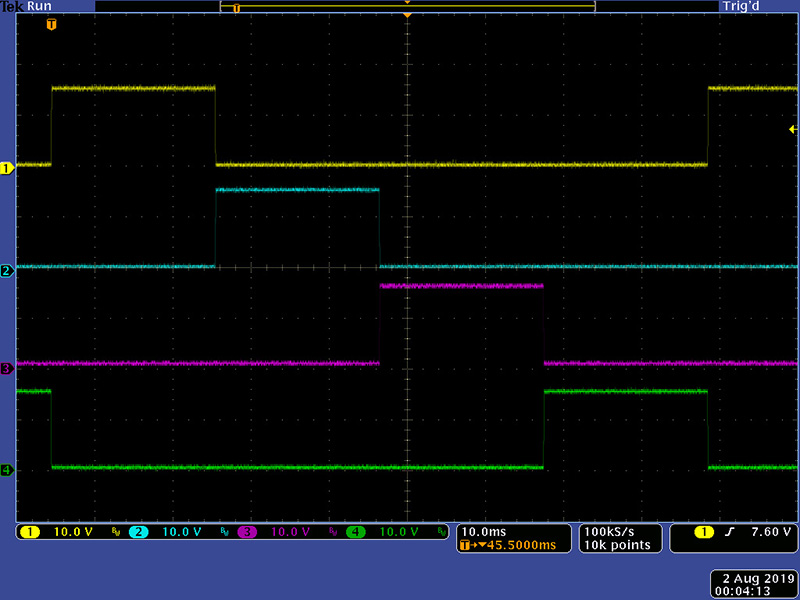
This photo shows the Pulse, Reference, and two channels of output.
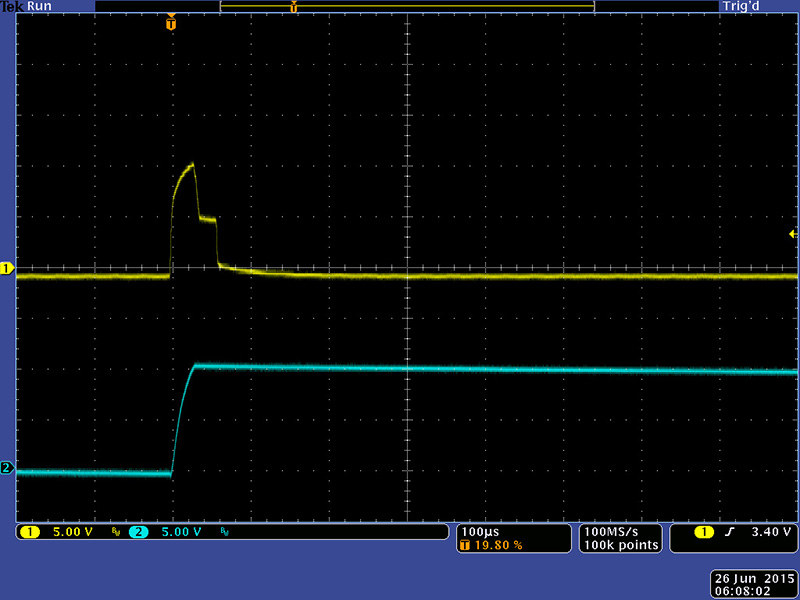
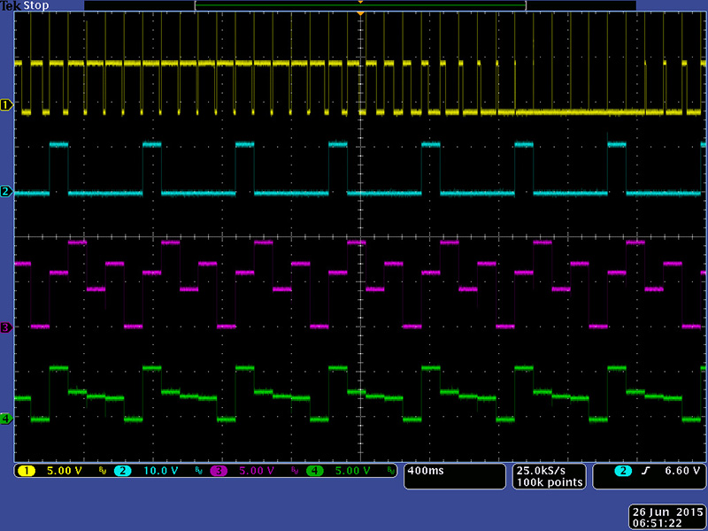
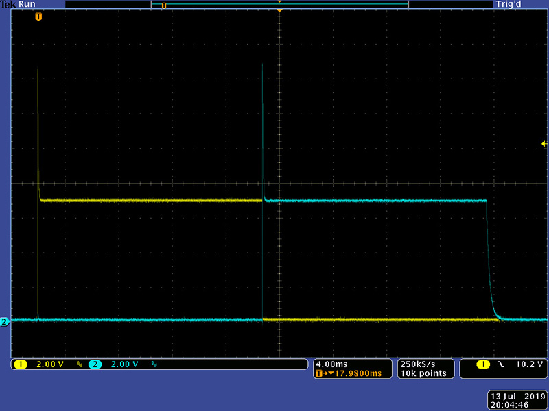
This scope image shows modulation of the pulse length (e.g. gate) time.
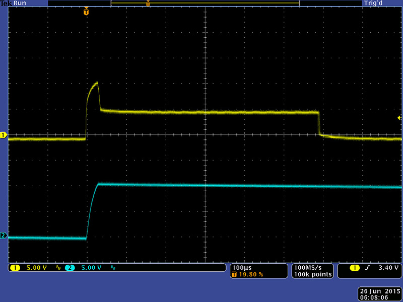
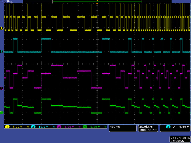
This scope image shows modulation of the intenal time.
Calibration
There are just two trimmers. TR1 sets the clock frequency so I calibrated for 2 Hz at the 0.5 knob setting.
TR2 sets the tracking of the Analog input. This takes a bit of explanation. First, the values used in the BOM are different from the original. Second, the notes on the schematic for the 245 and 246 conflict.
The Analog input over-rides the pulse input. Therefore, 0V input, as in nothing connected, would constantly select Stage 1. The Analog input has to be slightly positive to select Stage 1 which allows pulse operation with no Analog input. There is no trimmer and the top resistor is a 43K2 on the original schematic. The stage resistors are 1K with an 820R to ground. The current through the string is 312 µA. Stage 1 is selected when 0.25V < Analog in < 0.56 so Stage 2 is selected at 0.56V, Stage 3 is selected at 0.88V, Stage 4 is selected at 1.19V and Stage 5 is selected at 1.5V. These values see a bit odd to me.
I decided to have the stages selected on octaves, so 1.2V. For some margin, I selected 2 semitones less as the threshold. I wanted Stage 1 to be selected a bit lower than 0.25V so I chose 0.1V < Analog in < 1V so Stage 2 is selected a 1V, Stage 3 at 2.2V, Stage 4 at 3.4V, and Stage 5 at 4.6V. I changed R69 from 100R to 83R and R87 from 1K to 750R to adjust Stage 1. I changed R127 to 6K2 to set the range which sets the string current to 1.2 mA. I adjusted TR2 until the bottom pad of R127 was -4.6V. The reason for the negative voltage is the reference and the analog inputs are inverted at the comparators.
Modifications
The original 245 used a 24V supply and the logic was a mix of DTL and early TTL that ran from +5V. This redesign uses CMOS with a 15V supply and the 24V circuitry is simply driven from 15V with no compensating changes. In addition, a number of resistors were changed or added.
I modified a 245 and 246 with the "best" and my
customer's email back was "So the report is - they work flawlessly.
Null zone has been reduced to almost nil, adjacent stage pulse outputs
now individually trigger the 281's - even three/four in a row.
I encountered no problems with the stage trapping - either open ended on
either side or between two mid-points.
Stage CV Input
There are two unused CMOS gates with inputs floating and the stage CV op-amp is not rolled off which adds to the system noise. To correct the Stage CV input make these modifications:
PCB2:
Connect pins 1,2,5, 6, and 7 of IC14 together (this grounds unused inputs).
Add a 100 pF capacitor across R71.
I list two modifications to reduce the control dead zone and increase the output. The first helps some but the second corrects the operation entirely. To correct the Stage CV output make one set of these modifications.
Stage CV Output Level better
The maximum CV output is 9.4V at 3 o'clock. From 3 o'clock to full CW there is no change in CV output. To increase the CV output level and decrease the dead zone make these modifications:
PCB1:
Remove R178, R180 R182, and R184 (note PCB1).PCB2:
Change R150, R152, R154, and R166 to 150K.
R151, R153, R155, and R167 were 470K and changed to 150K. They are simple pull downs so you can leave as 150K.With these modification the maximum CV output is 14.4V at 4:30 o'clock. From 4:30 o'clock to full CW there is no change in CV output.
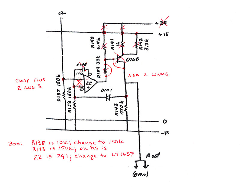
Stage CV Output Level best
The 741 is being over-driven so there is a very minor dead zone at the very end of rotation. The way to correct this without using 24V to drive the 741 and output buffers is to replace the 741 with a rail-to-rail LT1637 op-amp. The transistor buffer is no longer required so you can eliminate it. The buffer amplifier was an inverter so feedback is taken to the + input of the op-amp. Without this inverter you need to swap the + and - inputs to the op-amps. I chose to lift pins 2 and 3 and wire but you can also cut runs.
PCB1:
Remove R178, R180 R182, and R184 (note PCB1).PCB2:
Change R150, R152, R154, and R166 to 150K* (or 330K - see * below).
R151, R153, R155, and R167 were originally 470K and changed to 150K. They are simple pull down resistors so 150K is fine.
Remove C24, C25, C26, C28.
Remove R135, R136, R137, R138, R139, R140, R141, R142, R143, R156, R157, R158.
Remove Q31, Q32, Q33, Q34.
Connect the base to the collector with a link on Q31, Q32, Q33, Q34.
Replace R144, R145, R146, R161 with a link.
Replace IC15, IC16, IC17, IC18 with LT1637.
Swap pins 2 and 3 of IC15, IC16, IC17, IC18.*All four channels measured ~50 mV offset at CCW. This offset voltage depends on matching the voltage drop of the diode feeding "a" and the feedback diode. This offset can be trimmed by increasing the value of the pull down resistor on the - input of the op-amp. I found that a 330K resistor worked reasonably well in decreasing the offset down to around 10 mV.
This is the schematic of the CV output modifications:
With this rail-to-rail op-amp modification the output levels now go to +15V with no dead zone. This scope image is showing all four outputs going to +15V in a four step sequence.
Stage Pulse Output Level
The stage pulse outputs are 14.4V 8 µS trigger with a 10.8V gate (the yellow is stage 1 which has been modified for the lower gate voltage as described below).
To correct the stage pulse outputs make these modifications:
PCB2:
Change R61, R67, R79, R85, R94, R100, R109, R115, R124, and R131 to 6K8.
The resulting stage pulse outputs are 14.8V 80 µS trigger with a 7V gate (the cyan is the stage 2 pulse which shows minor cross talk).
This image is the stage 1 and 2 pulse outputs both with 100K loads.
This image shows stage 1 and 2 connected together with a 100K load. The trigger remains nearly 8V in amplitude and will now trigger a 281 when multiple stage gates are connected in parallel.
Clock Waveshape
Once I modified the five pulse output levels stage one would no longer trigger stage 2. Stages 2-5 functioned correctly. This design is an asynchronous state machine and the clock is very critical. Looking at the clock output was already on my list to do. This is the clock on the node connecting R163 and R174. Their ratio determines the clock amplitude. The falling edge has some noise and undershoot.
I replaced R160 with a trimmer and adjusted it to eliminate the clock pulse undershoot which restored normal operation to stage 1. I replaced R163 and R174 with a trimmer to be able to adjust the clock amplitude. I tweak both of these until I get stable operation.
PCB2: Updated
Change R160 to a 10K trimmer.
Remove R163 and R174. Move R173 to the front of the PCB to make room for the
trimmer. Cover the top pad of R173 on the rear to insulate it. Mount the trimmer
with the wiper in the bottom hole of R163. The CW side should just reach the top
of R163 and the CCW side will need to be lengthened to reach the bottom of R174.
Mount the trimmer slightly off the PCB to clear pads and traces.
You should be able to adjust the two trimmers to get a clock
that looks like the cyan trace which provides stable operation. I measure this
on the top lead of Q24. I have sometimes seen oscillations after the pulse
before it settles to the flat line. This can come and go with various settings
of the CV output controls. I've added a 100 pF capacitor on the front from the
bottom pad of R163 to the bottom pad of R172 to eliminate these oscillations.
I've worked with a number of people by email with issues on their 245. Some found they had to do the diode modification and this slightly different and easier modification to the clock wave shape.
PCB2:
Change R163 and R174 to 10K trimmers
Adjust R174 for a baseline of 2V. Adjust R163 for an 8V amplitude above the
baseline.
Note this matches the clock baseline in the above photo.
The diode modification issue is documented on my 246 Sequential Voltage Source Module in the Epilog. You have to lift the end of the resistor and capacitor that connect to the collector of the transistor. Bend the parts to connect the leads together and add either a Schottky or signal diode with the anode in the pad from either the resistor or capacitor. Wire the cathode to the lifted parts. These are in order of the stages. If you think you have this issue, you can always modify 2 or 3 stages and see if normal operation is restored for them.
| Stage | Resistor | Capacitor | Transistor |
| 1 | R61 | C9 | Q11 |
| 2 | R80 | C12 | Q15 |
| 3 | R94 | C15 | Q19 |
| 4 | R109 | C18 | Q23 |
| 5 | R124 | C21 | Q27 |
A customer sent me information on which leads to lift. Click on the image to see a full size PDF.
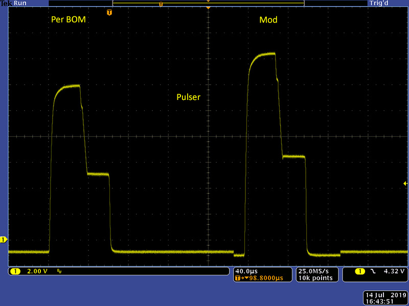
Pulser Output
The original design was a 13.5V short trigger followed by a 7V gate. The additional attenuation makes the output level sensitive to loading. To correct the pulser output make these modifications:
PCB2:
Change R175 to a link/wire.
Remove R176.
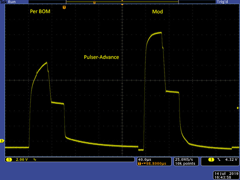
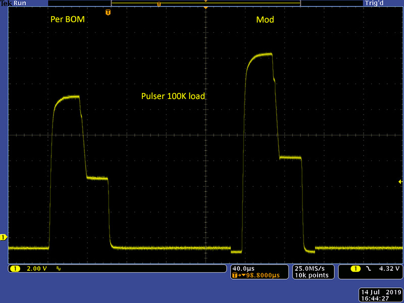
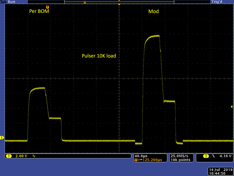
These next scope images are combined before modifications (Per BOM) and after modifications (Mod). The modified Pulser output with no load increases amplitude of both trigger and gate.
The Pulser output when connected to Advance decreases in amplitude but the modified Pulser output maintains amplitude.
The Pulser output when connected to a 100K load decreases in amplitude but the modified Pulser output maintains amplitude.
The Pulser output when connected to a 10K load decreases significantly in amplitude but the modified Pulser output decreases just slightly.
Reference Output
The Ref output was driven by 24V and is reduced in amplitude from the original. The additional attenuation makes the output level sensitive to loading. To restore the reference output to near 15V make these modifications:
PCB1:
Change R48 to a link/wire (note PCB1).
Remove R49.
Final Observations
These modifications have improved the performance of the 245 significantly. There are two idiosyncrasies that remain.
I can select a single stages by turning off all the switches and pulsing the Stage Select input. Using the switches I can only reliably select stage 1. If I try to select any other single stage either stage 1 is selected or other stages will come on. I have verified this on multiple 245s so I believe it is inherent in the design.
When a single stage is selected the pulse output is attenuated. This seems reasonable since the stage is retriggering itself in an asynchronous fashion.
This is PCB2 with these modifications.
PCB2 modifications photo (larger PDF)
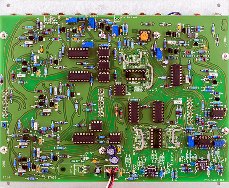
245 cj3000/V3 Modifications
There is a previous version 245 that I believe was sold at ElectricMusicStore initially. It has "245 Core V3" and "cj3000" in silk screen on the rear.
I had a module to repair where the pulser rate was very erratic. I found significant oscillations on IC15, a LS318 dual pair. A 100 pF capacitor across pins 2 to 3 tamed the oscillations and resulted in a well behaved clock.
These are the modifications to improve the stage pulse output and CV levels on this version.
Stage CV Input
PCB2:
All unused CMOS gates have their inputs grounded so no modifications required.
Add a 100 pF capacitor across R66.
Stage CV Output Level
PCB2:
Change R142, R147, R154, R161 (all 10K) to 330K.
Remove C31, C32, C33, C34 (all 33pF).
Remove R138, R84, R150, R157 (all 1K), R139, R88, R151, R158 (all 3K3), R140,
R145, R152, R159 (all 6K8)
Remove Q35, Q36, Q37, Q38.
Connect the base to the collector with a link on Q35, Q36, Q37, Q38.
Replace R141, R146, R153, R160 (all 33K) with a link.
Replace IC11, IC12 with LT1638. (corrected)
Swap pins 2 and 3 of IC11, IC12; swap pins 5 and 6 of IC11, IC12.
There are no series resistors for the CV outputs so I replaced the wire to the banana jack on PCB1 with a 1K series resistor and wired the second banana jack to the first.
Stage Pulse Output Level
PCB2:
Change R8, R20, R32, R44, R56 (all 47K), R9, R21, R33, R45, R57 (all 22K) to 6K8.
Clock Waveshape
This version includes trimmers for the clock waveshape.
Pulser Output
No modifications required.
Reference Output
No modifications required.
This photo shows the components removed and only the links installed so the reference numbers can be seen. The reference number for R147 is obscured by sleeving since there is a run underneath. Note C34 is under IC12. The components to be modified have a transparent red overlay. The three resistors with the transparent yellow overlay were moved to the opposite side of the PCB to allow access to the IC pins to solder wires to swap the pins as I chose to not cut traces on this PCB. The missing ICs and components outlined in orange are a trimmed buffer for the four stage CV outputs which have been bypassed. Since there is a CV level dead zone there really is no value in adding these components.
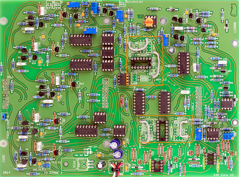
High resolution image of 245 cj3000/V3 PCB2 modifications
245 cj3000/V3 PCB2 Reference Diagram
Here is the final modified 245 V3
SAModular 245
I changed a few parts from the BOM. The Stage LEDs are dim so I decreased the series resistor from 4K7 to 620R for R57, R75, R90, R105, and R12. These would probably benefit from using a more efficient SSL-LX5093SID LED.
I used a SSL-LX5093SID for the red Stop LED and a SSL-LX5093USBD for the blue Start LED. Both are quite efficient so increased R1 and R50 to 33K.
I used C&K 8125SHZBE pushbutton switches for Start and Stop since I could get red (801803000) and blue (801807000) caps. These switches do NOT have a compatible pinout. The Stop switch needs the top and middle pads swapped with the NC terminal at the bottom. I cut the runs on the front of the board and ran wires to swap the pads. The Start switch just needs the NC terminal at the bottom.
The SAModular 245 incorporates all my modifications into V1.1 boards. How pleasant it is to be able to just build the PCB without having to do so many hand modifications.
Calibration is straightforward. I adjusted TR1 for 2 Hz at the 0.5 legend. I adjusted TR2 for 2V stage selects, and I adjusted TR3 and TR4 for reliable clocking between stages. I ended up adjusting TR4 to full CW and TR3 for a nicely shaped square top on the pulse measured on TP1.