 |
Barton Dual Quantizer Module replaces |
|
I wanted a quantizer and also a lag function so I combined them both in the DJB-013 design since there was adequate panel space. Since I built this module I have acquired a Blacet MiniWave and my ComputerVoltageSource modules which all have quantizing functionality and the MOTM-820 VC Lag Processer so my DJB-013 Quantizer and Lag module is redundant. I decided to replace it with the Barton BMC-016 Dual Nice Quantizer which has 16 different quantizing modes. There is a thread on the Electro-Music forum on the BMC016 Dual Nice Quantizer. Note this is for the six trimmer version, not the 8 trimmer version.
Barton Dual Quantizer
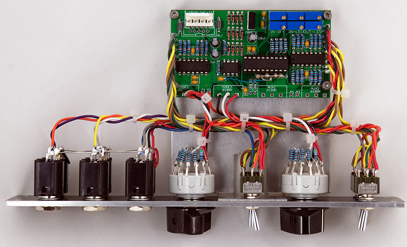
The Barton BMC016 PCB is very compact and has part values silk screened on it.
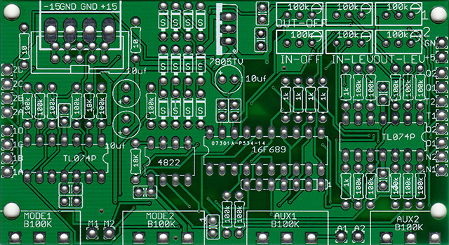
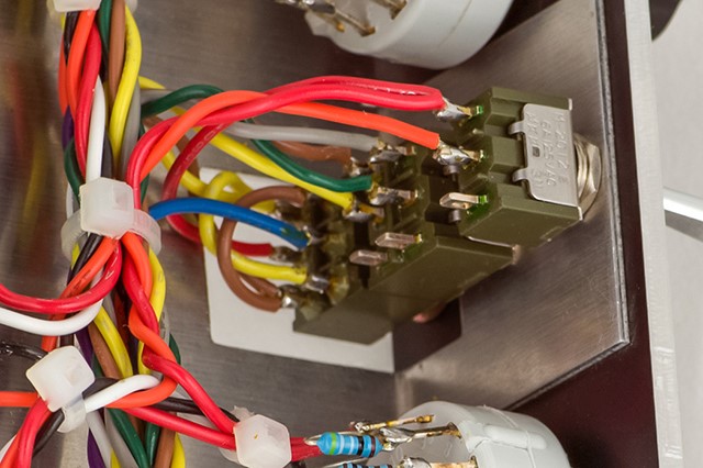
I did not install the 100K resistors for the Aux1 and 2 inputs.
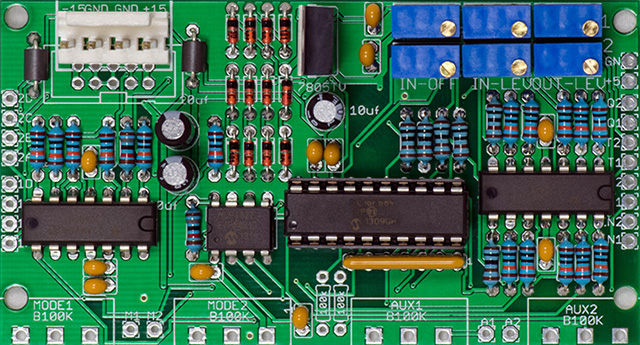
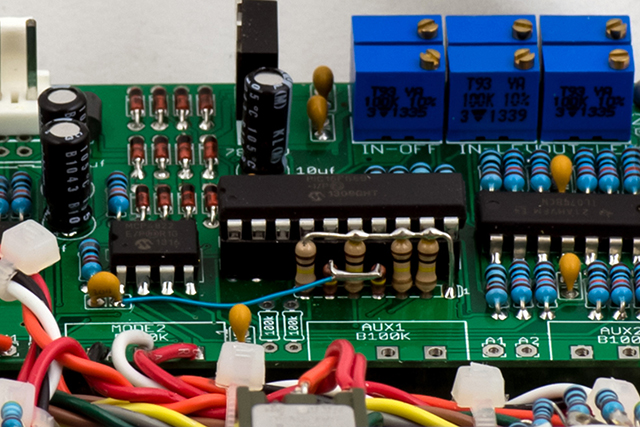
I wanted the module to fit in a 1U panel so I did not use the Aux input and attenuator. I wanted precise mode selection so I replaced the Mode control with an 8 position switch. I pulled the T1 and T2 inputs to +5V instead of ground with 100K resistors (the above photo still shows the resistor network) and used a center off switch to selects a single input jack for Trigger, Bypass, or Quantize. This photo shows the resistor network. I used 1/8W resistors for the pullups so they would be shorter and I could bend the leads out for wiring.
The spacing is very tight between the two DPDT switches. I chose NKK because they fit the spacing. Other switches may be wider so be sure to check. Note also I had to notch the bracket around the one switch as there is not enough clearance on the outer edge of the switch for a bracket.
Originally I though about using the unused Aux input to add a half a semitone to each channel (replace the 100K Aux input resistors with 2M4 to +5V ). This would allow a quantized input to quantize to the same value instead of possibly to the next lower semitone. However the software works quite well on a quantized input with no issues - great!
I made a 0.050" aluminum bracket with a cutout for switch clearance. I mounted the bracket with the three center switches as the 8 position switch bushings are just a bit too short. This module was somewhat difficult to assemble due to the number of wires and the small size of the PCB. The wire pad spacing would not accommodate 0.100" connectors.
| Power Consumption | |
| +15V | -15V |
| 23 mA | 16 mA |
Barton Dual Quantizer modifications
I couldn't keep the switches and controls on standard MOTM spacing came up with a pretty good compromise (left). Synthcube has since released a slightly modified version of this panel in a single color (right).
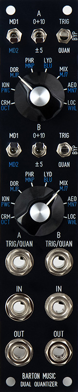
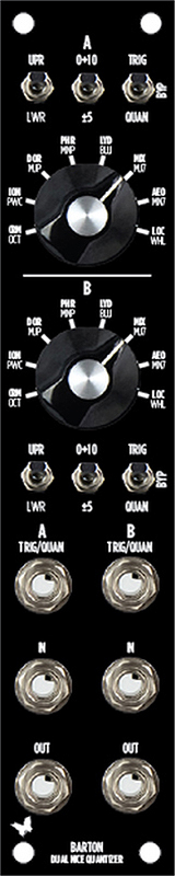
Barton Dual Quantizer FrontPanelExpress design file
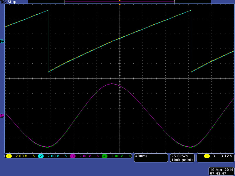
This scope image shows channel A and B in Bypass mode. In Bypass mode the time between steps, or the conversion time, is 4.2mS. The voltage steps consequently become greater as the dV/dT increases. At this slow rate of change the output is quite accurate.
This scope image shows channel A in Octave mode and channel B in Chromatic mode. The chromatic steps are too small to see in at this vertical resolution.
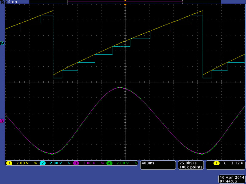
This scope image shows channel A in Octave mode and channel B in Ionian mode.

This scope image shows the Trigger mode where the input is only quantized when the Trig input is high.
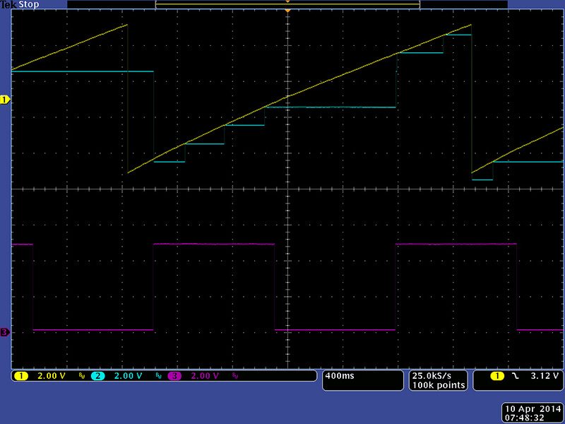
This scope image shows the Quantize mode where the input is quantized when the Quant input is high and is bypassed when the Quant input is low.

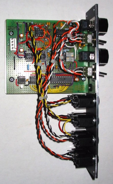
DJB-013 Quantizer and Lag
I started with an ARP-style quantizer design that I found on Chris List's CV Quantizer site. I modified this design with a better clock oscillator and a parallel counter. I also improved the sample clock generation on the rising edge of the comparator. I added 1/2 semitone voltage and hysteresis to the input so that quantized notes would quantize to the same value (e.g. 0 volt input quantizes to 0 volts). For the lag circuit I wanted both a linear and exponential lag. I change the time constant between the two responses for a similar effect.
I shortened a MOTM-000 prototype board for building this module.
DJB-013 FrontPanelExpress design file
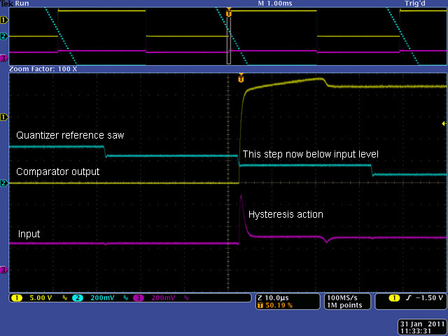
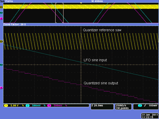
The seven bit counter and DAC form a 128 step ramp waveform with each step equal to 78.1 mV. This ramp is inverted, offset, and scaled through the two op amps to form a saw (e.g. ramp down) waveform with each step equal to 83.3 mV (middle trace). The input (top trace) is compared to the saw waveform and the comparator output (bottom trace) goes high when the saw is lower than the input. The input to the comparator is increased by ~1/2 semitone and hysteresis is added from the comparator output which can be seen in the small steps in the input waveform. Adding ~1/2 semitone assures that notes that are already quantized will be quantized to the same value. The hysteresis assures a clean comparator output for any noise on the input.
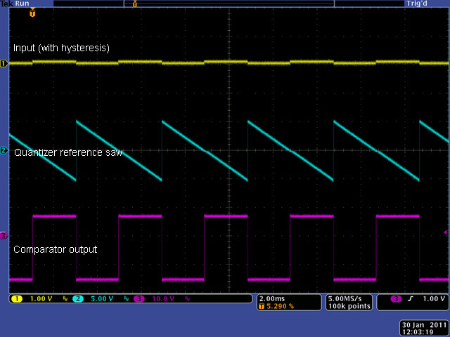
When the reference saw goes below the input, the comparator switches state. The value of the reference saw is the quantized value of the input.
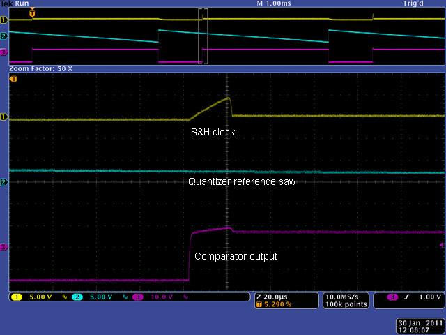
The rising edge of the comparator is processed by a transistor circuit to generate ~5 µS pulse to sample the reference saw to provide the output. The input comparator, pulse generator, sample & hold, and output buffer are duplicated for the second quantizer channel.
This scope image is the quantizer operating on a LFO sine wave input. You can clearly see the quantized steps in the output waveform.
To calibrate the module:
Remove the offset jumper and adjust the voltage at the op-amp pin 1 to -5.333 volts.
Move the gain jumper to the alternate position and adjust the voltage at the op-amp pin 14 to -10.583 volts (gain of -1.066).
Replace the offset jumper and move the gain jumper back. Adjust the offset control very slightly to get as close to 0 volts on the quantizer module output with no input.