|
Buchla Timbre & Crossfader PCB |
|
I built the Aaron Lanterman adaptation of the Buchla Music Easel Timbre & Crossfader. Aaron's information on the PCB is on his Lantertronics Timbre and Crossfade page.I bought the Rev 1 PCB which corrects several of the Rev 0 issues.
Timbre & Crossfader Rev 1 Schematic (published with permission from the Aaron Lanterman site)
Timber & Crossfader Rev 1 Mouser Parts List
I updated Aaron's documentation for the changes to Rev 1.
Timber & Crossfader Rev1 Updated Documentation (published with permission from the Aaron Lanterman site)
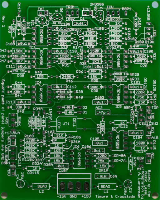
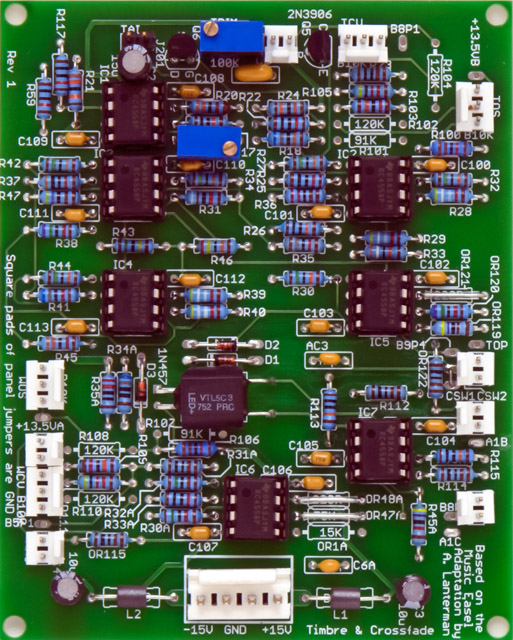
Timbre & Crossfader Rev 1 Components
I updated the schematics with my modifications and indicated the parts not used.
Timbre & Crossfader Rev 1 schematics with modifications
Timbre Modifications
I found that the input voltages were way to high for my circuit. Upon looking at the Buchla schematics I believe R19 is 3K3, not 33K. This lowered the input signals much closer to an acceptable level so I added an input trimmer to fine tune it. Too much input and it starts morphing, too little and the output is low. I modified the timbre circuit for 5V CV and audio inputs and outputs and to use 100K potentiometers.
|
Timbre Modifications: All modifications are detailed on schematics with modifications TAO changed to 5
volt pk-pk output: TAI
changed to 5 volt pk-pk input:
TCVI changed to 5 volt input: TOS
changed for 100K potentiometer: |
I was able to use MTA connectors for all IO except for TAI which uses straight square pins. You can see the additional R17 trimmer to adjust the input level. I didn't find that the filter switch made much difference so I shorted CSW1 to CSW2 on the PCB.
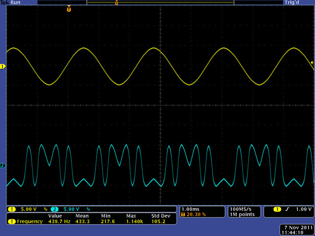
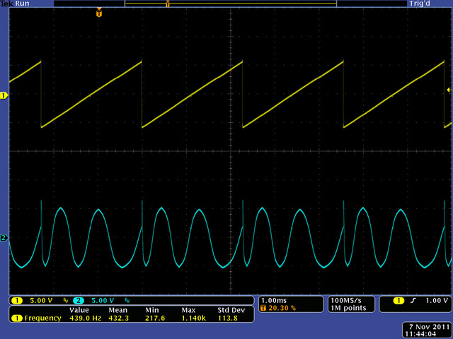
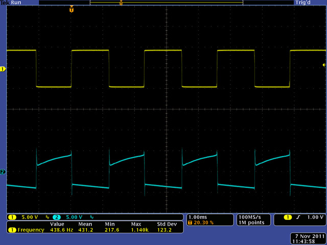
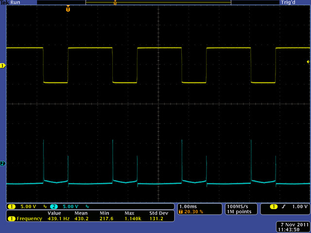
Timbre Waveforms
This image shows the timbre wave folding of a sine input.
This image shows the timbre wave folding of a ramp input with the same offset setting.
This image shows the timbre wave folding of a square input with the same offset setting.
This image shows the timbre wave folding of a pulse input with the same offset setting. I just adjusted the pulse width to achieve this output which has significant DC offset. I AC coupled the output with a non-polar capacitor at the jack to eliminate the DC offset.
Crossfader Modifications
Similar to the Timbre circuit, I modified the crossfader for unity gain, 5V CV input and to use 100K potentiometers. I found that I could only partially crossfade to A2I as A1I bleeds through to the output. I changed R45A to balance nearly complete crossfading with distortion. This value is dependant on the characteristics of the vactrol used.
|
Crossfader Modifications: All modifications are detailed on schematics with modifications MXO
to unity gain:
WCVI changed to 5 volt input: WOS
changed for 100K potentiometer: |
Crossfader Waveforms
This image shows the crossfader with R45A at 4K7. You can see the incomplete crossfading to A2I (ramp) as A1I (sine) bleeds through to the output.
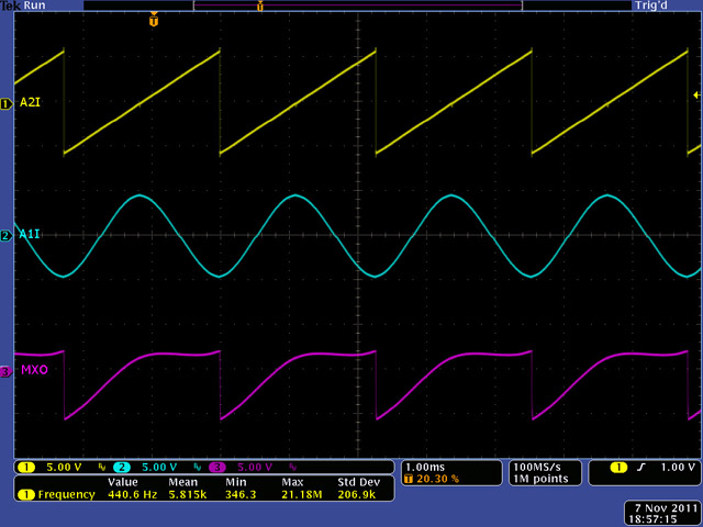
This image shows the crossfader with R45A changed to 49K9. You can see complete crossfading to A2I (ramp) with minimal distortion. A 47K to 49K9 value is a reasonable compromise between complete crossfade and mimimal distortion for the VTL5C3 vactrol that I used.

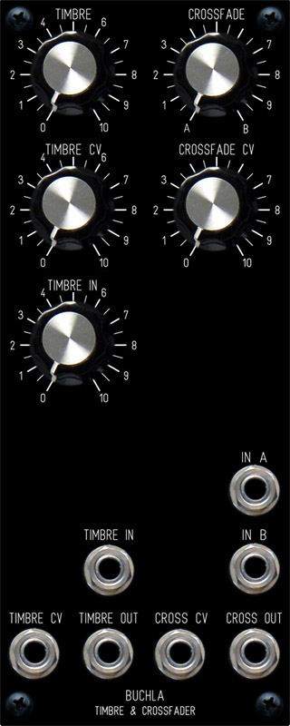
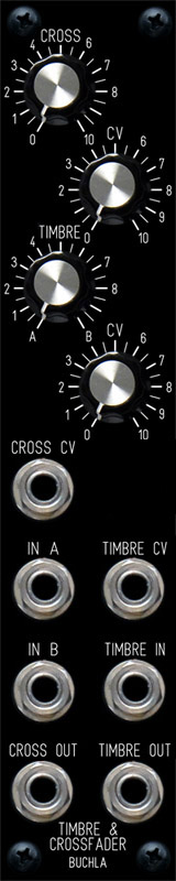
Panel
Here are three concept panels. The design on the left uses small knobs to fit in a 1U width panel. The right design adds a Timbre In attenuator since the input level is critical to proper operation of the timbre generator.
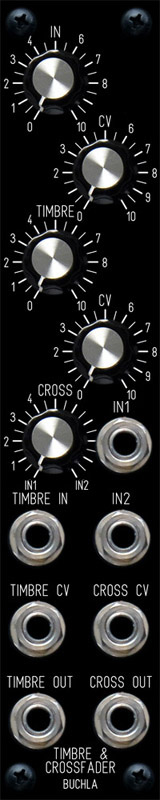
This design uses standard MOTM knobs and spacing in a 2U panel. I decided to combine the Timbre & Crossfader with the Pulser in a single 2U module.